Single Ended vs Differential Signals and How OrCAD X Aids in Design
Key Takeaways
-
Compare differential signals and single-ended traces in high-speed PCB design.
-
Additional considerations for layout and routing with differential pairs.
-
See how OrCAD X aids in managing EMI and signal integrity in Ethernet and USB designs.
High-speed ethernet design requires special attention to be paid to stackup and impedance.
In days past, if you used a telephone that was plugged into the wall you could hear conversations from others bleed into your phone line. Today, high-speed PCB design uses differential pairs to solve these types of signal integrity problems. Differential pairs are the primary routing style used with high-speed digital signaling protocols, including standard computing interfaces like USB and networking interfaces like Ethernet.
The differences between single ended vs differential signals are simple at the physical layout level, but they can be complex at the signal level and in terms of driver/receiver component functions. Read on as we discuss the intricacies of this method. Mastering differential single ended vs differential signal pair routing will provide the foundational knowledge needed to design ethernet, USB, and others’ differential impedance correctly, to promote signal integrity.
Single Ended vs Differential Signals — Considerations for Layout and Routing
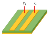
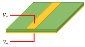
|
Differential pairs |
Single-ended |
|
|
Impedance |
- Characteristic and differential impedance specified. |
- Only characteristic impedance is specified. |
|
Definition |
Uses two traces carrying equal and opposite signals to improve noise immunity and signal integrity. |
Uses one trace and a reference ground, simpler but more prone to noise interference. |
|
Length matching |
- Required between each trace in a pair. |
- Only needed for parallel buses or to match with a source-synchronous clock. |
|
Signal readout |
|
|
|
Receiver termination |
Parallel termination between pairs (high Z). |
Shunt termination to the ground plane (high Z). |
|
Example signaling standards |
USB, Ethernet, RS-232, RS-485, HDMI |
I2C, SPI, GPIOs |
What Are Single-Ended and Differential Signals?
Single-ended and differential signaling are two methods for designing PCB traces. Today, digital interfaces are standardized to use one of these methods of signaling. Low-speed protocols in general use single-ended signaling while high-speed protocols use differential signaling, although some low-speed protocols still use differential signaling. These two types of signaling and routing can be used with various topologies.
-
Single-ended signals are fairly straightforward: The HIGH level is brought up to a logic level (5 V, 3.3 V, etc.) and the LOW level is defined as zero or ground.
-
In differential pairs, each trace in the pair carries the same magnitude, but opposite polarity. At the receiver, the signal is recovered by taking the difference between the signal levels on each line.
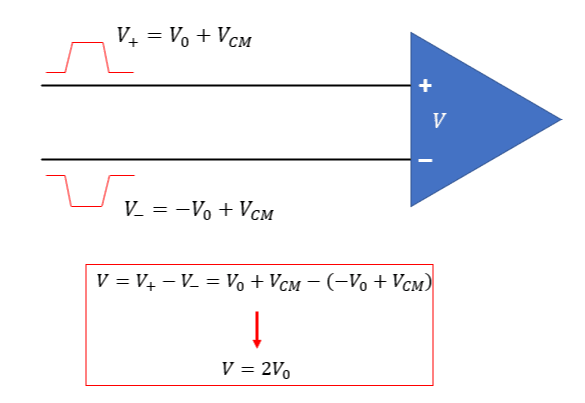
Differential signal recovery at a receiver component.
Differential Signals in Depth
In differential signals, successful readout and signal recovery requires the lengths of the pairs to be impedance matched within some small tolerance. If done correctly, common-mode noise will be canceled when reading the signal, as shown in the conceptual diagram above. Ethernet differential impedance matching, like other differential pair length matching, prevents reflections in the lines that undermine power delivery and contribute to poor signal integrity.
The signal readout and recovery process for differential pairs account for the fact that the two pairs carry equal and opposite polarity signals. This simple idea and parallel routing in a differential pair solve some important signal integrity problems in high-speed PCB design.
Impedance Matching for Differential Signals
Impedance matching (also known as length matching) is an important design aspect of differential signal design. As outlined, the signal recovered at the receiver is intended to be twice the magnitude of either individual trace. However, alternating signals are not static; instead, they fluctuate between peaks and troughs over some period. When arriving at the receiver, the signals must be perfectly out-of-phase to maximize power delivery.
Because the arrival time is dependent on the length of the trace travel, the signals must be the same length to achieve this out-of-phase condition at the receiver. Although there is some tolerance in designs as to how much the signal length can diverge, most applications will result in a need to add back the missing length lost on the shorter signal from being on the inside turn. When adding back the missing length, care should be taken to lengthen at the location in the trace where the divergence occurs - the idea being that the more of the distance the traces have in common, the more likely they are going to experience the same local effects of impedance in the plane at that specific area.
Layout for Differential Signals
Layout for differential signals does not differ immensely beyond that of a critical single-ended trace. Within reason, component placement should bend to the differential pairs in the case where circuitry may cause EMI issues. Avoid placing power circuitry like switching regulators too close to differential pairs, as the effects of induction will be pronounced. Similarly, routing across split planes should be avoided at all costs due to the extreme EMI issues caused by a circuitous return path.
Ethernet Differential Impedance Applications Offer Routing Solutions
When looking through high-speed signaling standards, differential pair routing is predominantly used. Differential pairs are useful for two major reasons:
-
Common-mode noise - A differential pair is read out as a difference in signal level between the two pairs at a receiver. In other words, any common-mode noise will be subtracted from the receiver and will not interfere with the received signal. This includes common-mode crosstalk that might be received from a single-ended signal.
-
Inconsistent reference - Differential pairs don’t need a uniform ground plane to provide controlled differential impedance. Instead, the pairs reference each other. Interestingly, by calculating the Z-parameters for a differential pair, it becomes apparent that the self-impedance and coupling impedance both diverge to infinity, but the difference between these is a constant.
The image below shows a driver and receiver stage used in low-voltage differential signaling (LVDS). Here, there is no ground plane surrounding the pair. Because the signals have equal magnitude and opposite polarity, the electric field terminates on each side of the differential pair. This particular diagram is nice because it illustrates the situation seen in a standard like Ethernet over UTP cable (e.g., Cat5), which may not have any grounding in a significant portion of the interconnect.
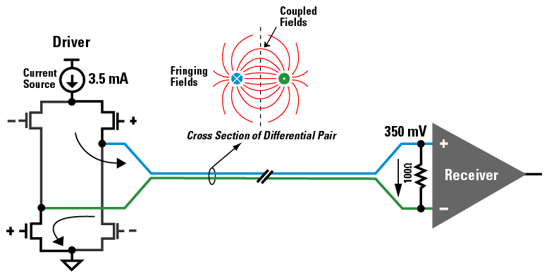
Example differential channel with LVDS
In this example with LVDS, the receiver end is terminated with 100 Ohm impedance, which is equal to the pair’s differential impedance. This eliminates reflection in the differential signal at the receiver end. Because differential receivers have high input impedance, the terminator is placed in parallel with the inputs, converting the injected current into a voltage that can be recovered at the receiver.
What Differential Signals Don’t Solve
It’s important to note that differential pairs are not a cure-all for every signal integrity problem. A differential pair can experience some of the same signal integrity problems as single-ended traces, but they manifest in different ways. Here are the broad signal integrity problems experienced by differential pairs.
|
Phenomenon |
Description |
|
Differential-mode noise/crosstalk |
Contrary to popular belief, differential pairs produce crosstalk and are vulnerable to crosstalk. Differential crosstalk between pairs can interfere with signal recovery at the receiver. |
|
EMI reception |
Differential signals can still receive radiated EMI from external sources, but only differential-mode noise affects the receiver. |
|
EMI emission |
Differential pairs emit electromagnetic radiation that can be received as common-mode noise in other interconnects, though the emission is weaker due to opposite field polarities in the pair. |
|
Signal distortion |
As signals travel along interconnects, they experience losses and dispersion, leading to signal distortion, which affects both differential and single-ended signals. |
Reference Planes
In both types of signaling, a reference plane near the traces helps solve one problem—it provides shielding against EMI. It also provides a place for some return current around a trace by allowing field lines to terminate into the reference plane. The reference plane also defines the single-ended impedance (characteristic impedance) for each trace in a differential pair as well as in a single-ended signal. Routing tools can enforce length matching in your differential pairs while maintaining controlled impedance during routing.
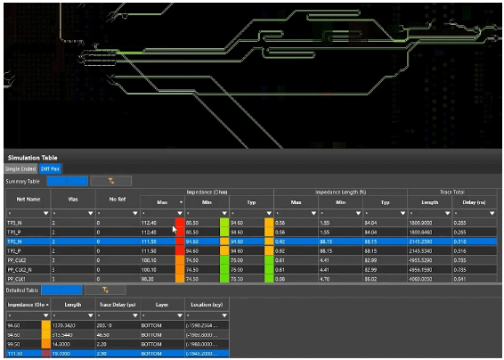
OrCAD X allows you to do signal analysis and see the individual impedance breakdown of specific parts of nets.
Working With OrCAD X for Differential Signals
|
Challenge |
OrCAD X Capability |
Explanation |
|
Impedance Control |
Impedance Workflow in Signal Integrity (SI) Analysis |
OrCAD X allows impedance control for differential pairs by running an impedance analysis workflow, ensuring the layout meets the required differential impedance for high-speed signals like USB, Ethernet, and HDMI. Impedance tables show single-ended and differential impedance values. |
|
Length Matching for Differential Pairs |
Constraint Manager for Differential Pairs |
The constraint manager allows designers to define length matching constraints for differential pairs. This ensures equal length traces for the signals, preventing timing mismatches that could cause signal degradation. |
|
EMI Emission and Crosstalk |
Via Arrays and Shielding Tools |
OrCAD X supports adding via arrays, which can help shield differential pairs and reduce EMI and crosstalk by ensuring that the signal return paths are managed effectively, preventing noise coupling. |
|
Signal Distortion Due to Impedance Mismatch |
Real-Time DRC for Impedance and Length Matching |
Real-time design rule checks (DRC) help detect mismatches in impedance or length during layout. If there is a mismatch in differential pair impedance or length, OrCAD X generates an immediate error, allowing designers to correct the issue before finalizing the design. |
|
Routing Across Planes |
Layer Stack-up and Reference Plane Management in Cross-Section Editor |
OrCAD X provides tools to configure the layer stack-up and manage reference planes, which are essential in controlling the impedance of differential pairs. Ensuring proper return paths across planes reduces the chances of EMI and cross-talk. |
|
Differential Signal Recovery |
SI Analysis for Differential Signals |
OrCAD X can run signal integrity (SI) analysis on differential signals to simulate the signal recovery at the receiver, checking for signal degradation, noise, and impedance mismatches. This analysis ensures that differential signals are correctly interpreted at the receiver. |
|
Termination Issues |
Workflow Manager for Impedance Analysis |
OrCAD X provides workflows to check for termination issues in differential pairs, such as mismatched terminations or reflections that can distort signals, ensuring the correct resistive terminations are placed in the design. |
Now that you know the difference between single ended vs differential signals, you can use Cadence PCB design and analysis software to accurately design your project. Ensure your signals, differential or single-ended, adhere to your requirements with OrCAD X advanced routing tools —you’ll have everything needed to create high-quality designs in a single application.
Leading electronics providers rely on Cadence products to optimize power, space, and energy needs for a wide variety of market applications. To learn more about our innovative solutions, talk to our team of experts or subscribe to our YouTube channel.
