Differential Signaling Demystified
source: wikimedia
It’s common knowledge that the digital world is made up of 1’s and 0’s. When a PCB designer builds a circuit to send data from point A to point B, that data signal is mapped to a voltage high (often 3.5 to 5 volts) and a voltage low (often 0-volt ground). This simple signal architecture is called a single-ended signal and is the most common way to transfer an electrical signal from sender to receiver.
But while single-ended signals are great for most general purpose applications, there are many cases where the rise and fall times between voltage highs and voltage lows start to become a bottleneck in your design. As the demand for higher data rates increases, PCB designers are increasingly turning to differential signaling architectures to overcome the limitations of single-ended designs. Read on to learn what differential signaling is and how it can be used in your PCB designs.
What is differential signaling?
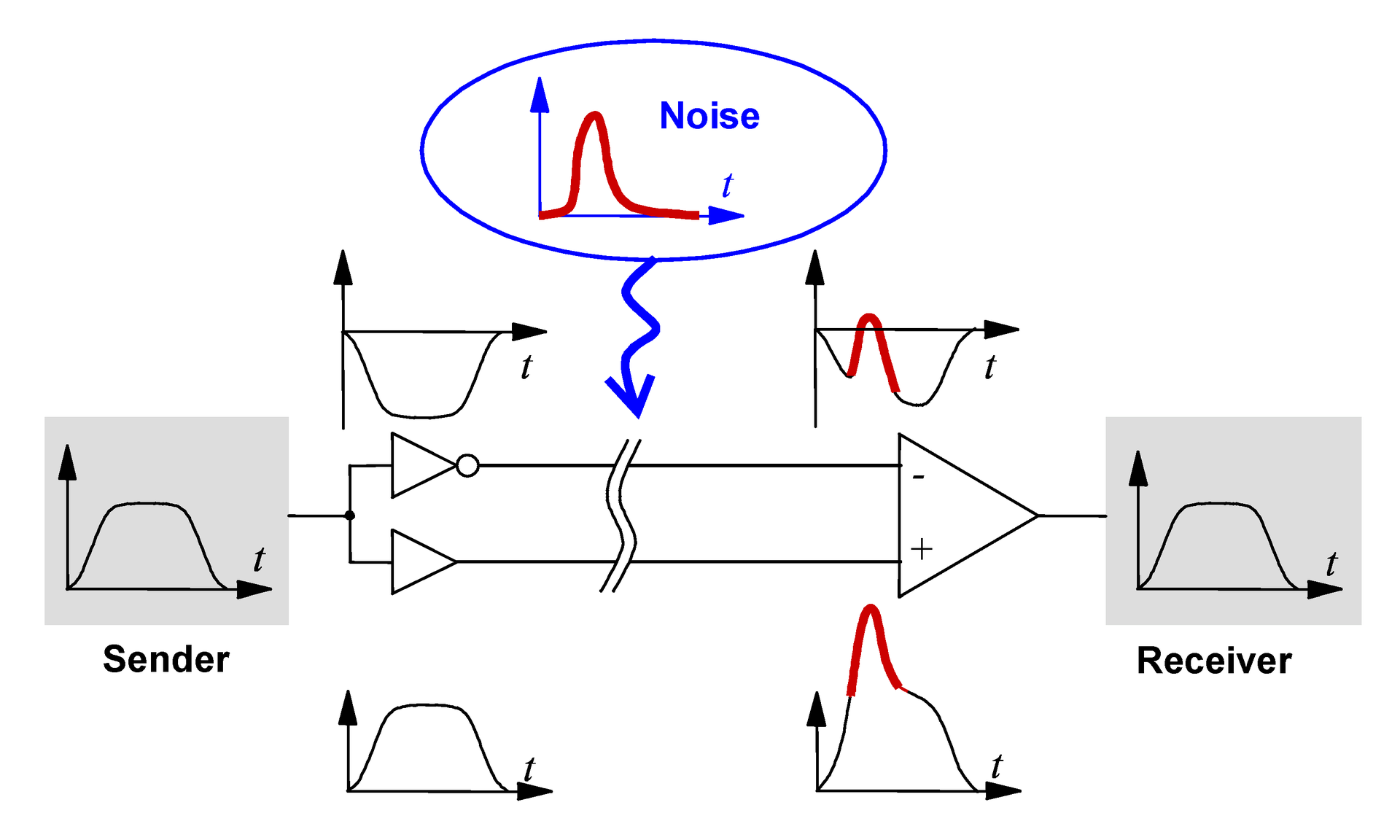
Differential signaling involves using two voltage signals, one positive and one negative to create one information signal. One voltage line is paired with an inverted signal that is identical in amplitude but opposite in polarity relative to a common-mode voltage. It’s the difference between the voltages of the two voltage lines that give you the 1’s and 0’s that make up your data signal.
Pros of differential signaling
The faster you can switch between voltage high and voltage low, the faster the data rate. The primary advantage of using differential signaling is the fact that it reduces the voltage amplitude that you would see in a single-ended signal. A smaller amplitude leads to shorter rise/fall times, which translates to a faster data rate.
Furthermore, even though differential signals are not immune to EMI or crosstalk, they are able to evenly distribute the noise and interference between the positive and negative signals, helping minimize the impact.
Here’s a quick summary of the pros of differential signaling:
-
Smaller amplitude, shorter rise/fall times, faster data rate
-
The return currents of the two voltage lines cancel out
-
Helps minimize EMI and crosstalk
-
Smaller voltage amplitude means lower operating voltage requirements and reduced power consumption
-
Precise logic gate timing
Cons of differential signaling
There’s really only one major con of differential signaling, but it is a pretty big one—you need twice as many conductive paths to provide a differential signal as you do for a single-ended signal. Space and cost requirements can impact the feasibility of using a differential pair in your design.
Common applications of differential signaling
The convenience of modern living owes much to differential signaling, these are just some of the most common applications:
-
Ethernet
-
USB
-
HDMI
-
LVDS (Low-Voltage Differential Signaling)
-
Balanced audio for high-quality sound recording and production.
Best practices for routing differential traces in PCBs
Now that you’ve seen how useful differential signaling can be, here are some quick tips for implementing the technology in your designs:
-
Keep differential traces parallel and closely coupled for best EMI performance
-
Keep width, thickness, and impedance constant across differential traces to maintain signal integrity
-
Keep differential pair conductors as far away as possible from neighboring signals to avoid interference
-
Keep the length of each line in a differential pair equal
It’s generally a good idea to also refer to any layout recommendations that come with the manufacturing specifications that accompany the drivers and receivers you are trying to use. For more general recommendations, you can refer to technical standards such as RS-485 for drivers and receivers in serial communications systems, and RS-422 for digital signaling circuits (often used to extend RS-232 connections).
Conclusion
In summary, if you can afford to use differential signaling within your PCB designs, it’s possible to reap the benefits of higher data rates, lower power requirements, and reduced EMI noise. At the same time, the use of differential signaling architectures also adds complexity to your circuit design. This is why it’s important to use EDA (electronic design automation) tools to analyze and understand how voltage, impedance, and signaling are affected by your PCB layout. Check out Cadence’s suite of PCB design and analysis tools today.