OrCAD X Constraint Manager
Key Takeaways
-
The Constraint Manager includes all the rules for design layouts to ensure high performance, manufacturability, and reliability.
-
The DRC can actively or manually check the design for violations using the ruleset defined in the Constraint Manager.
-
Users can further define custom sets of nets or regions of the board to tweak the ruleset to the design’s requirements.
The OrCAD X Constraint Manager guides performance and manufacturability during layout.
The world of PCB design offers an infinite number of design possibilities. While this can be freeing with experience, a design, more often than not, needs constraints to realize and execute the engineering team's design intent properly. The OrCAD X Constraint Manager guides PCB design by ensuring designers are aware of layout and manufacturing issues with live updates. Before starting the layout, every designer should configure constraint settings for a rapid and seamless transition from design documents to manufacturing files.
OrCAD X Constraint Manager Guide Analysis
|
Solutions |
Benefits |
Applications |
|
|
|
How Constraints Help Designers and Manufacturers
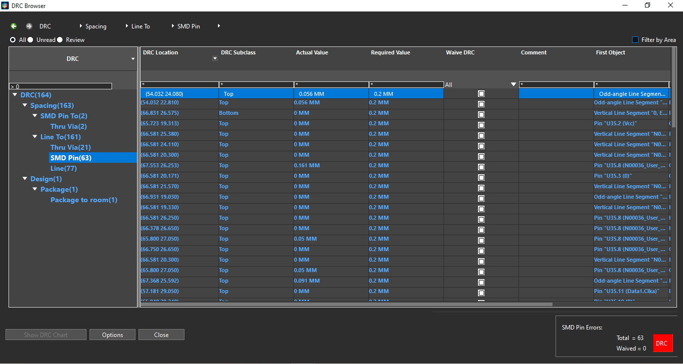
The DRC browser shows violations in the design according to the rules set in the Constraint Manager.
Constraints act as both a boundary and a flag for the designer to prevent unnecessary resources spent on a design that is unproducible or financially infeasible to manufacture. The design rule check (DRC) is the hub for the different constraints in the design across various domains (electrical, physical, spacing, 3D, etc.) The DRC offers a live and batch method of checking the design:
-
Live DRC actively assesses board objects to determine violations; the board canvas automatically shows the offending flag whenever a violation occurs. For most layouts, designers prefer an active DRC to catch potential design flaws as they occur for quicker resolution.
-
Batch DRC is a manual process initiated by the user, typically at the end of the design or any point where considerable changes to the current design may occur. It is less flexible than a live DRC and is primarily a remnant of bottlenecks in workstation processing power. However, it can still be helpful for exceptionally large, intricate, and dense designs.
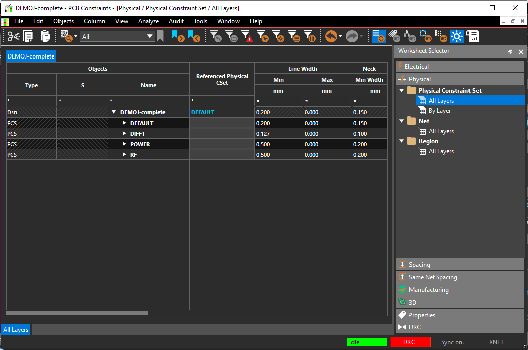
The DRC is a byproduct of the Constraint Manager. Users can quickly navigate to its location from the OrCAD X design canvas by locating Tools > Constraint Manager in the top navbar.
Breaking Down OrCAD X Constraint Manager Domains
Different design rules use a domain organization by their defect discipline to keep the Constraint Manager organized:
-
Electrical - Electrical constraints mainly control the performance of a signal during its transmission to prevent degradation or a deviation from expected performance/function. Some key areas:
-
Net/trace topology
-
Signal timing/propagation delay
-
EMI management
-
Power integrity
-
-
Physical - Primarily concerned with the aspects of the PCB that affect fabrication and assembly processes, i.e., stackup design, through-holes, via structures, component placement, board dimensions, and more. Physical constraints maintain the performance of the board throughout the various production stages. Examples include:
-
Board outline
-
Component placement rules
-
Differential pair geometry
-
-
Spacing constraints - Indicate the minimum distance between certain features or objects of the board, like traces, components, and the board edge. These prevent manufacturing issues by providing ample space that exceeds equipment operating precision and prevents shorts while limiting the effects of EMI. These include:
-
Trace-to-trace clearance (different and same-net)
-
Component-to-component clearance
-
Trace-to-board edge clearance
-
Pad-to-pad spacing
-
-
Manufacturing constraints - To ensure manufacturability, constraints are necessary to prevent board design from exceeding the capabilities of current technology. Observing manufacturing constraints makes it far more likely that the manufacturer pushes a design back for revisions. Some constraints are:
-
Hole sizing
-
Solder mask and silkscreen clearances
-
Copper pour rules (hatching, thermals, etc.)
-
High-speed design - As digital signal rise/fall times become significantly faster with continued innovations in chip design, boards have to compensate for the potential lossy nature of signal transmission. Some rules include:
-
Via stitching for return current
-
Signal rise time
-
Additional Constraint Manager Customization Options
Rule definitions apply globally between objects, i.e., a common trace-to-trace spacing across the board. However, sometimes the design needs to bend the rules to accommodate the performance better; this rule-bending occurs under careful consideration of the overall impacts on the manufacturability to the board. Moreover, the one-size-fits-all approach to design rules can be limiting even when manufacturing is a concern. For this, designers can create and customize net classes, net groups, and regions:
-
Net class - A group of similar nets within the same domain, i.e., power, data, etc.
-
Net group - Like a net class, but with cross-domain functionality.
-
Region - A defined board area where local design rules supersede global rules.
While the approach is similar between these custom rulesets, their functionality and application differ slightly:
Comparing Net Classes, Net Groups, and Regions
|
Benefits |
Examples |
|
|
Net Class |
|
|
|
Net Group |
|
|
|
Region |
|
|
Cadence Solutions for Complex Layouts
The OrCAD X Constraint Manager guide gives design teams a quick overview of the built-in tools and extensive customization options for designers to realize complex layouts quickly. Interested in learning more about the new OrCAD X platform? Check out the complete list of Cadence PCB Design and Analysis Software to see how we’re helping designers realize today’s and tomorrow’s electronic devices.
Leading electronics providers rely on Cadence products to optimize power, space, and energy needs for a wide variety of market applications. To learn more about our innovative solutions, talk to our team of experts or subscribe to our YouTube channel.