How To Use the Constraint Manager In OrCAD X
Key Takeaways
- Use the Constraint Manager in OrCAD X to set and apply physical and spacing constraints for consistent PCB designs.
- Understand how to create Constraint Sets (CSETS) for different nets, improving design efficiency and reducing manual input
- Discover the process of exporting and importing technology files in OrCAD X to maintain standardized design rules across multiple projects
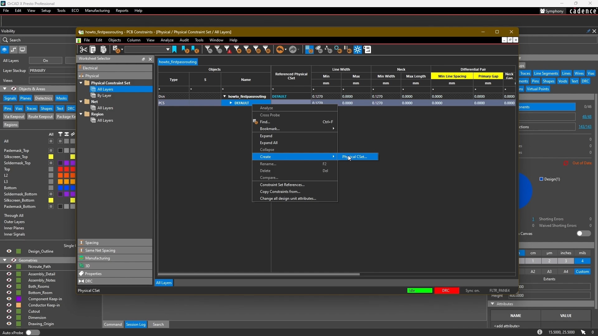
Through the constraint manager, CSETS are applied to different nets or regions in the design. The image shows how to create a new CSET.
Many companies establish a default set of PCB constraints or rules to apply uniformly across all their designs. In OrCAD X, this is accomplished through the constraint manager, which covers aspects such as track thickness for signals and power, spacing between lines or pads, differential pair guidelines, and matched length requirements.
OrCAD X users can create and save technology files (*.tcfx) that include the necessary layer and rule information for standardized PCB design. Using the Constraint Manager in OrCAD X ensures that your design will meet the predefined constraints as you create it, reducing the need for revisions later. Read on as we discuss how to use the Constraint Manager.
Goals For This Tutorial
To begin, go to Tools > Constraint Manager. Constraint Manager is a comprehensive tool for managing all design constraints. Goals for this tutorial are:
- Trace Width Constraints: We'll set constraints for different trace widths, like wider widths for power traces and narrower for signal traces. Complex designs with differential pairs will require appropriate widths and spacings.
- Spacing Constraints: We'll set constraints to control the spacing between different traces or copper features in our design.
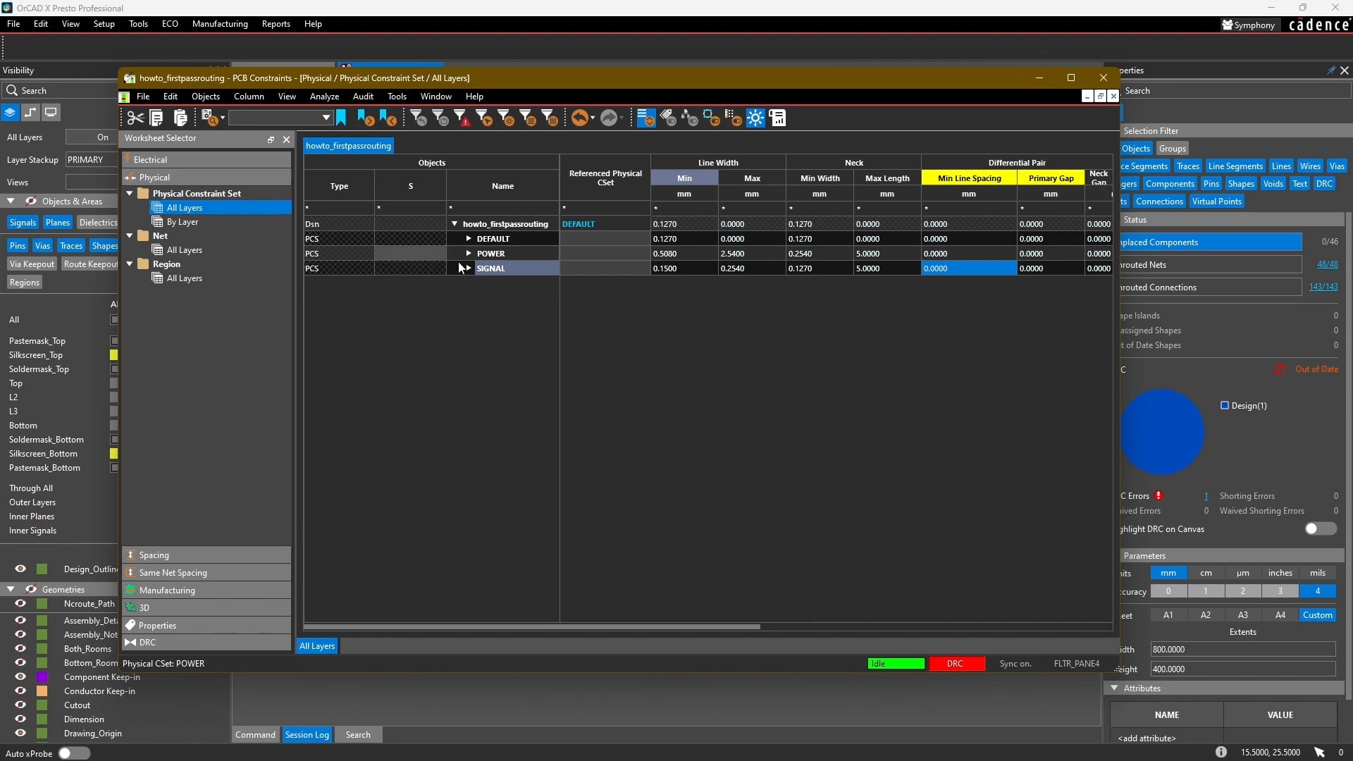
Two physical CSETS for power and signal. Yellow column headers mean the rule is off, and can be changed by right-clicking on it.
How to Use Constraint Manager Physical Constraints
Constraint Sets (CSets) are predefined rules that can be applied to various nets or regions in your PCB design. They streamline the design process by allowing you to define a set of constraints once and reuse them throughout your design. This method ensures consistency and efficiency, preventing the tedium of manually entering constraints for each net. You edit a CSET and then apply it to different nets or regions within your design rather than manually configuring parameters for each net.
The following example demonstrates how to set up constraints for power signals in a PCB design using OrCAD X. This example specifically considers a power signal with an arbitrary minimum amperage of 5A and arbitrary layer stackup thickness of 1.6mm. These settings ensure that the design meets the necessary current capacity and signal integrity requirements
|
Step |
Action |
Details |
|
1. Creating Constraint Sets |
Navigate to Physical Constraint Sets. |
|
|
2. Setting Line Widths |
Expand the constraint set to set values for line width and neck. |
|
|
3. Creating Signal Constraints |
Follow the same steps to create a set named "Signal." |
|
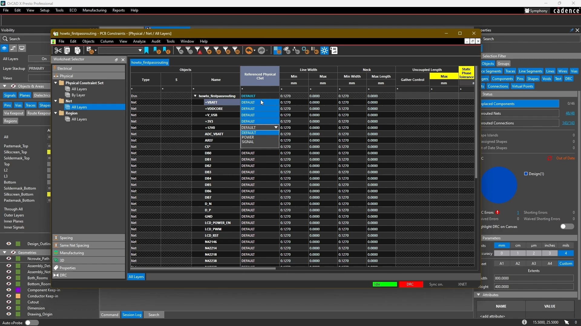
Assigning the spacing constraint sets in OrCAD X
Assigning Constraint Sets
Once you've defined your CSETs, head into the Nets section where all nets in the design are listed. If you do the work upfront, you can group them into buses and other groups, allowing you to set a CSET for multiple nets at once instead of individually. Highlight the nets in the Physical Constraint Set section, then select the appropriate CSET from the dropdown menu.
- Navigate to the Net section.
- Assign the "Power" constraint set to power nets like +VBATT, +VDDCORE, etc.
- Assign the "Signal" constraint set to other signal nets.
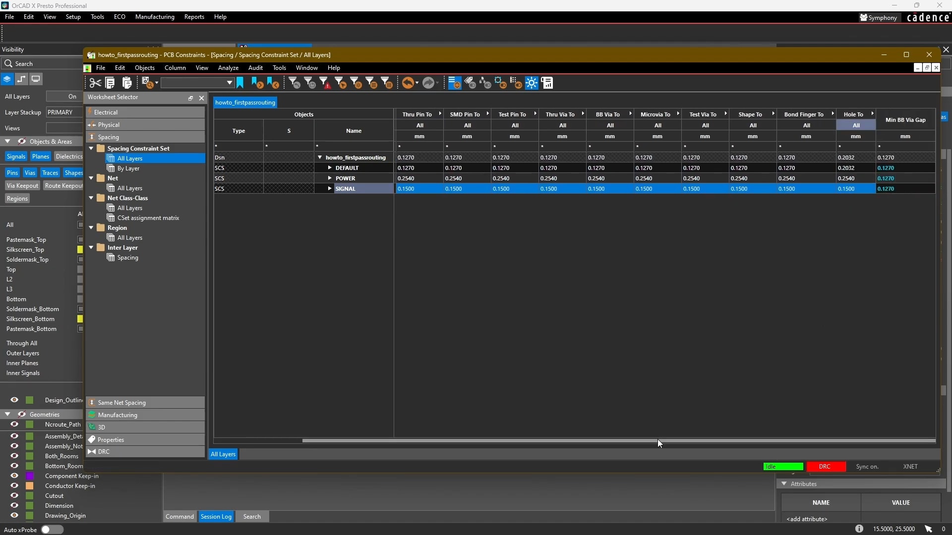
Setting “line-to-all” spacing as 0.15 mils by setting the first cell and then copy-pasting it into the remaining ones.
Spacing Constraints
Spacing works similarly in that you define a CSET and then assign it to different nets, classes, regions, or interlayer spacings.
Setting up spacing constraints is essential to ensure that the various elements in your PCB design have adequate separation, preventing electrical interference and ensuring proper functioning. In this section, we will create spacing constraint sets for both power and signal nets and assign these constraints to the appropriate nets in our design.
|
Step |
Action |
Details |
|
1. Creating Spacing Constraint Sets |
Go to the Spacing section under All Layers. |
|
|
2. Setting Spacing Values |
Set spacing for the "Power" constraint set. |
|
|
3. Setting Spacing Values |
Set spacing for the "Signal" constraint set. |
|
|
4. Assigning Spacing Sets |
Assign the "Power" and "Signal" spacing sets to the appropriate nets. |
|
Finalizing Constraints and Additional Rules
In addition to setting basic constraints, you can specify via lists for power and signal traces by double-clicking in the via list section and selecting the appropriate vias. Use the Analysis Mode to enable or disable specific rules by right-clicking on the headers and selecting Analysis Mode. After setting constraints, refresh DRCs to check for errors and make any necessary adjustments. This organized approach ensures efficient constraint management and consistency in your PCB design.
Exporting and Importing Technology Files in OrCAD X
Use File > Export > Technology File, specify an output filename, and click Save. You can control the file's contents, including the cross-section, constraints (electrical, physical, and spacing), user property definitions, and manufacturing constraints. To import a technology file into a PCB Editor Board file (.brd), open Constraint Manager and use File > Import > Technology File and browse for the .tcfx file. You can import the technology file in Merge, Replace, or Overwrite mode, with Overwrite enabled by default.
Understanding how to use the Constraint Manager is essential for any PCB designer aiming for precision and efficiency with OrCAD X. Explore Cadence's PCB Design and Analysis Software and learn more about OrCAD X to enhance your PCB design workflow today.
Leading electronics providers rely on Cadence products to optimize power, space, and energy needs for a wide variety of market applications. To learn more about our innovative solutions, talk to our team of experts or subscribe to our YouTube channel.