PCB Spacing Design Rules
Key Takeaways
-
Common PCB routing challenges, including trace width and spacing constraints.
-
How proper spacing improves signal integrity and board manufacturability.
-
The role of Allegro X constraint manager in setting up design rules.
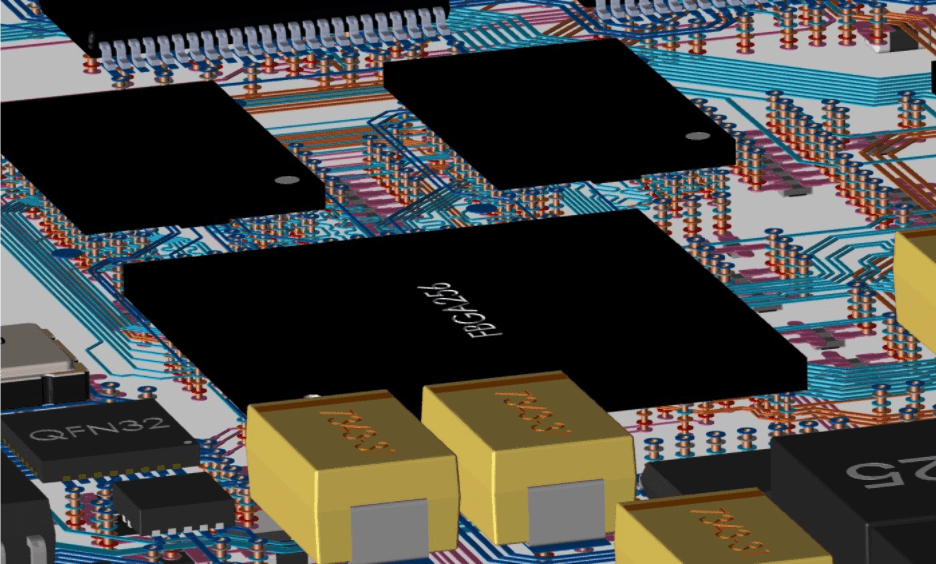
A multi-layer circuit board showing the routing on the internal layers.
In modern day PCB layouts, each net may have different and unique routing characteristics that have to be applied in order for the board to function as designed. In addition to specific areas that nets can be routed in or layers that they can be routed on, there are also different PCB trace width and spacing rules that have to be managed, as well. For this reason, creating proper PCB spacing design rules before routing and layout is foundational to a well-designed PCB.
We’ll discuss common challenges for circuit board routing, as well as methods for successfully routing while adhering to PCB spacing design rules and constraints.
Common Challenges in Today’s PCB Routing Technologies
Routing traces on a printed circuit board was once simple, with default widths and spacing, except for wider power and ground connections. However, as circuit board technology advanced, trace width and spacing requirements became more complex. In addition to these trace width and spacing requirements based on the functionality of the circuit, there also may be different width and spacing requirements dictated by their location. Designers also must choose from an array of different via types and sizes for their routing.
PCB Spacing Design Rule Related Considerations in Modern Routing Technologies
|
Category |
Details |
|
Trace Width and Spacing Requirements |
- Controlled Impedance Routing: Specified widths and spacings. |
|
Width and Spacing Based on Location |
- Connectors: Smaller trace widths to fit between closely spaced pins. |
|
Via Type Selection |
- Thru-Hole: The standard via in circuit board design, mechanically drilled to go all the way through the board. |
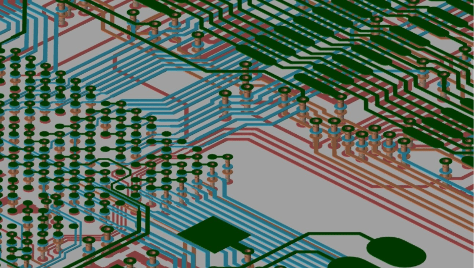
3D CAD layers showing the trace routing on a circuit board.
Examples of Routing and PCB Spacing Design Rules
PCB spacing design rules dictate the circuit board’s electrical performance, routing fabrication, and more. Here are four areas to consider when deciding what width and spacing values to use:
Electrical Performance and Signal Integrity
Most digital routing on a circuit board will use a default value for its trace widths and spacings, but some nets will require different sizes. Controlled impedance nets, for instance, will need their trace widths calculated based on the configuration of the board layer stackup. Sensitive high-speed traces may require larger spacing values to prevent crosstalk and other signal integrity problems.
Analog routing may also require unique trace widths and spacings depending on the purpose of the circuitry. In some cases, the default trace width may be reduced in tight and constricted areas, but care has to be taken that this isn’t extended across the board. If the trace gets so thin that it gets compromised during PCB fabrication, then the signal integrity of the entire board could be compromised.
Power and Ground Routing
Traces used to route power and ground need to be wider to conduct greater amounts of current. If the traces are too thin, they can get hot and even burn through. Power traces routed on the internal layers of the board also need to be wider for heat dispersal than those routed on the external layers, as exposure to the air will provide more cooling.
For those traces that are used in power supply circuitry, it is important to keep them as short and as wide as possible to handle the current, as well as to reduce inductance and noise in the circuit. It is important to increase the spacing for traces that are carrying higher current to prevent the power from arcing between them.
Circuit Board Fabrication
The wider a trace is, the easier it is to fabricate. The fabrication etching process will have a greater effect on traces that are long and isolated, so it is better to make them wider when possible.
-
A 20 mil trace will have a much greater tolerance for losing metal than a 3 mil trace would.
-
Trace widths are also dependent on the weight of the copper being used to build the layer of the board. If that layer of the board requires a greater copper weight due to higher current requirements, the fabricator may not be able to etch thinner trace widths on it as well.
Circuit Board Assembly
Traces that are too wide can affect how easily the components will solder during PCB assembly.
-
The wide traces used for power and ground nets can also act as a heat sink, leading to uneven heating and poor solder joints.
-
Small two-pin parts that are connected to a large area of metal on one pad and a thin trace on the other may be unbalanced enough that the component will be pulled up on end during solder reflow. This effect is known as “tombstoning” and will force manual rework of the board for corrections.
-
An abundance of metal under a BGA can also cause problems during soldering as well, but these errors are more difficult to find due to the size of the BGA on the board.
With all of the potential problems that can happen if the right trace widths and spacings are not maintained, PCB layout engineers need all the help that they can get. Fortunately, there are utilities in the design tools that can help with this.
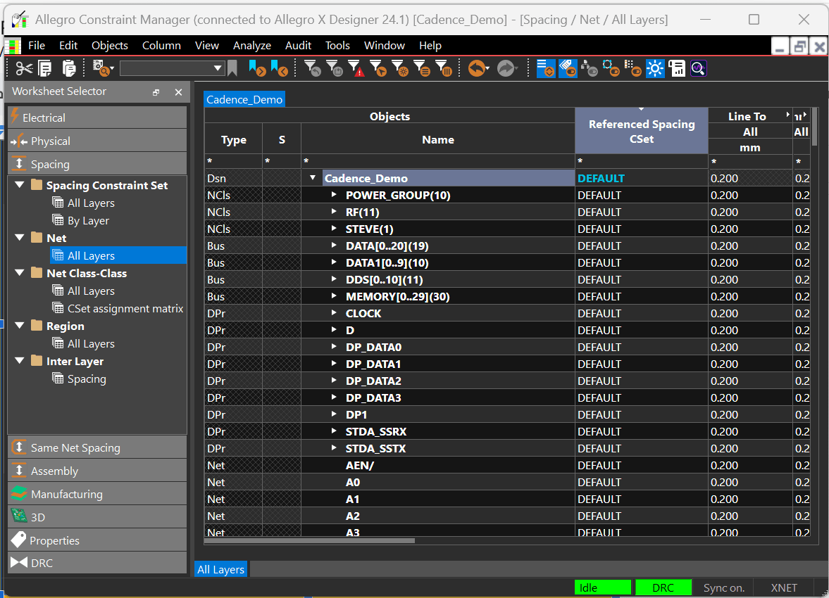
The design rules and constraints being set up for data net trace widths.
About PCB Spacing Design Rules and Constraints
Modern PCB layouts require managing various trace widths, spacings, and via assignments for individual nets, net groups (buses), and power/ground nets. Often, multiple sets of values may apply to a single net or group. PCB design tools handle this using design rules and constraint management systems.
Unlike early CAD tools with limited control, today’s constraint management systems offer spreadsheet-style interfaces to set rules for trace widths, spacings, via assignments, and more. They also manage signal timing, component spacing, and manufacturability settings like solder paste and silkscreens. In addition to constraint management, modern CAD tools provide advanced routing features to enhance design efficiency.
Working With Allegro X Constraint Manager to Create PCB Spacing Design Rules
To start defining your PCB spacing design rules:
-
Open Allegro X and click the Constraint Manager icon.
-
Since most spacing rules fall under spacing design constraints, select Setup Constraints → Spacing.
This opens the spacing worksheet, where you can enforce spacing (clearance) requirements between traces and components. If you want to apply spacing constraints to differential pairs, use the physical worksheet.
Creating a New Spacing Constraint Set
With the Constraint Manager open:
-
Navigate to the Spacing Constraint Set folder.
-
Right-click on your design name and choose Create Spacing Constraint Set.
-
Name your constraint set something descriptive, such as "10 mil Spacing Rule".
A meaningful name helps you remember that this rule is intended to maintain a 10 mil clearance between nets—a critical spacing parameter for ensuring proper electrical isolation and manufacturability.
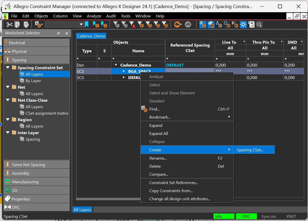
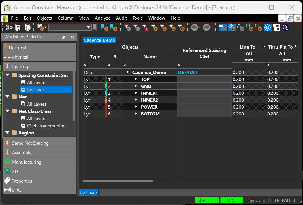
Creating a SpacingCSET in Allegro X Constraint Manager.
Defining the Spacing Rule
Now set up the specific spacing design rule:
-
Select “All Layers” within the spacing constraint set to ensure the rule applies across every conductor layer, including internal, top, and bottom layers.
-
Create a rule that enforces a 10 mil spacing.
In this example, the “10 mil” value is applied uniformly, meaning that all nets subject to this rule will maintain a consistent 10 mil clearance from adjacent elements. This consistency is key in PCB design to prevent shorts and ensure signal integrity. -
If the rule requires a necking value (a consistent taper or transition in spacing), set that also to 10 mil.
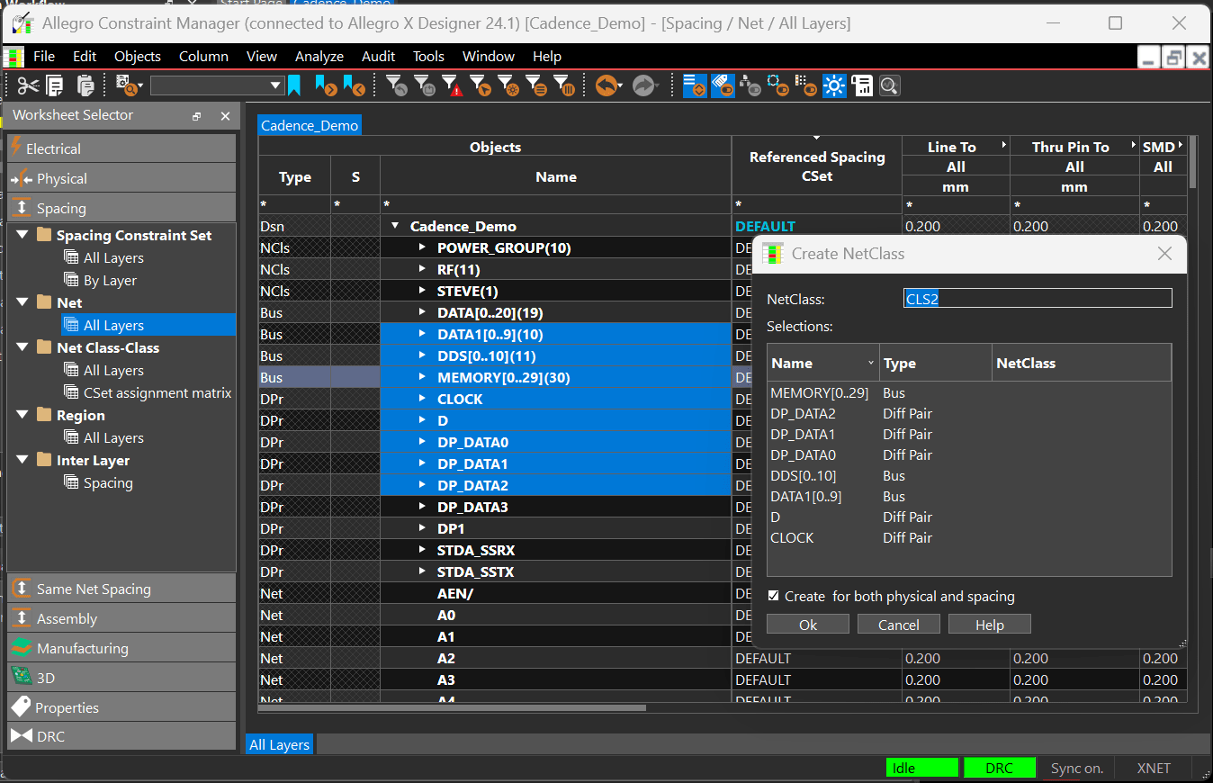
Applying the Spacing Rule to Net Groups
Next, you need to assign this spacing rule to the appropriate nets in your design:
-
Navigate to the Net folder within the spacing worksheet.
-
Click All Layers to view all the net objects.
-
Select multiple nets that need the same spacing rule. For instance, if several nets are labeled with a “Q” prefix (e.g., Q0 through Q7), select them all.
-
Right-click on any of the selected nets and choose Create Class.
-
Name this net class (for example, "Q Nets").
Grouping nets into a class simplifies the management of design rules and ensures consistency across related signals. -
Under the new net class, locate the Referenced Spacing Constraint Set cell.
-
Click the cell and choose your previously defined "10 mil Spacing Rule".
This action assigns the spacing rule to every net within the Q Nets class, enforcing the desired clearance automatically during routing.
Applying Rules to Individual Nets
If a specific net requires its own unique spacing parameter:
-
Navigate to that net (for example, an AEN net).
-
In its Referenced Spacing Constraint Set cell, simply select or type in "10 mil".
This direct assignment is useful when only one net needs the rule, bypassing the need for an entire net class. -
Similarly, if a net (like BNC2) requires a different spacing—say, 25 mil—enter that value directly in its cell.
Allegro X will then route that net with the specified spacing, overriding the default or grouped rule.
Verifying the Spacing Rule Application
To confirm that your PCB spacing design rule is active:
-
Zoom in on one of the nets (for example, one of the Q Nets) within the layout.
-
Use the Add Connect command to start routing.
-
As you route, observe that the net now displays the 10 mil spacing rather than the default value (often 9 mil).
This verification step confirms that the spacing rule has been correctly applied and is influencing the routing process as intended.
To learn more about how Allegro X can aid in ensuring your PCB spacing design rules are adhered to through the constraint manager, check out Cadence PCB Design and Analysis tools, and learn more about the Allegro X Design Platform.
Leading electronics providers rely on Cadence products to optimize power, space, and energy needs for a wide variety of market applications. To learn more about our innovative solutions, talk to our team of experts or subscribe to our YouTube channel.