How to Build Your Stackup in PCB Design Software
Key Takeaways
-
The importance of a good layer stackup in your PCB design and understanding the challenges in creating it.
-
What designers need to help them create the right layer stackup for their PCB design.
-
Tips on using your PCB design tools to create the best layer stackup configuration.
The side and top view of a dense PCB layer stackup
It used to be that PCB layout designers didn’t usually get involved with the planning of the layer stackup that would be used to build the circuit board that they were designing. They would obviously have to know the correct number of layers and their configuration in order to set up the design tools, but beyond that, they wouldn’t have any further interaction. This was due primarily to three reasons:
-
The performance requirements of the PCBs were not as exacting as they are today.
-
There were fewer materials available for the fabrication of PCBs.
-
The PCB design tools simply didn’t have the sophistication for board layer stackup and configuration capabilities that they do today.
Thankfully this part of the PCB layout process is now very different, as most major design tools are equipped with advanced PCB layer configuration features. That being said, it is still incumbent upon the designer to go through the process of configuring the right board layer stackup for their design. We’re going to take a look at this process and discuss some ideas for building and configuring board layer stackups in PCB design software.
The Importance of the Right Stackup in Your PCB Design
The number of layers in a printed circuit board was at one time tied directly to the number of nets that needed to be routed. As PCB circuitry requirements increased, so did the component count and ultimately the number of nets. At the same time, the active components were also growing in complexity and pin count, which drove up the net count on the board. The answer to these increases was to reduce the trace widths or increase the layer count of the board, or both, which unfortunately resulted in higher manufacturing costs.
While the average component and net counts on a PCB increased, so did the electrical performance specifications of the boards. Designers soon discovered that while six layers were now necessary to route what used to be a four-layer board, they would actually have to go to eight layers instead to get the electrical performance that was required. Some of the reasons for these additional layers include:
-
More room for isolated controlled impedance routing.
-
Differential pair routing restricted to as few layers as possible.
-
Microstrip and stripline board layer stackup configurations.
-
Additional plane layers for multiple power and ground nets.
As circuit board capabilities continued to evolve, yet another factor was introduced into the process of creating board layer stackups. The higher speeds that circuit boards are now operating at may require more advanced board fabrication materials then what has been used before. This is also true of very high-powered boards, or boards that will be used in harsh environments. These materials may alter transmission line characteristics of circuitry that were originally calculated for standard FR-4 material, which in turn may require changes in the layer stackup configuration.
With today’s advanced electronics, it is critical to create the right board layer stackup to ensure that the board will operate at its peak performance. And because of all the requirements that we’ve just explored, there is more pressure than ever on the layout designer to get the stackup correct. Let’s see what other difficulties that layout designers have to contend with.
Some of the Challenges for Designers in Stackup Creation
PCB designers face a lot of intricate challenges today that board designers in the past didn’t have to worry about. Do any of these sound like what you have had to deal with?
Schedules:
The need to get the product to market is more intense now than it has ever been before. Not only are corporations under more pressure to compete, but there are other forces at work too. Case in point, the recent COVID-19 outbreak caused a frenzy of medical design work in order to rush new medical devices into production to help fight the virus. And while all aspects of design feel the pressure to fulfill these needs, the PCB designer is especially challenged to get the board done quickly and without errors.
Information:
As we pointed out earlier, the demands for layer configurations and board materials become increasingly more complex every day. Many designers are not familiar with all of these processes or materials and need outside help to create the board layer stackup that will work best for what they are designing.
Tools:
Some PCB design tools are still not user friendly enough for a designer to use efficiently when creating their PCB layer stackups. Not only does this slow them down and add frustration to the job, but it also could impact how well a board is designed.
There are a lot of challenges that PCB layout designers face when trying to get their job done. This is especially true when trying to create a board layer stackup configuration to ensure the board works as expected while at the same time being able to manufacture it without error and at the lowest cost. Let’s look at some ways that PCB design tools can help designers.
Adding in the board stackup layers into a PCB board outline creation wizard
Layer Stackup Creation Assistance That Helps
There is a lot that PCB CAD tools can do to help the layout designer create and configure board layer stackups. The first is incorporating automated generators or wizards like what is pictured above. These allow a designer to specify layer counts and configurations for the stackup while the tools do the heavy lifting of creating it in the database. The next would be to give the designer total control over the layer stackup details including the ability to specify conductive and dielectric board materials. The designer should be able to specify values and tolerances as well as configure how the layers should be arranged when they set up the parameters of the layout.
However, not all of the help that a designer needs can come from the tools. There is a lot of industry knowledge that designers need to be able to better understand the materials and processes that they are working with. Here is where the designer could benefit immensely by developing relationships with their PCB contract manufacturers in order to get accurate information for creating their board layer stackups. As has been said, the manufacturers have been doing this job for years and years, and they are very good at it. Layout designers should be encouraged to engage early on with their PCB CMs in order to have the correct layer stackup before they begin their PCB design.
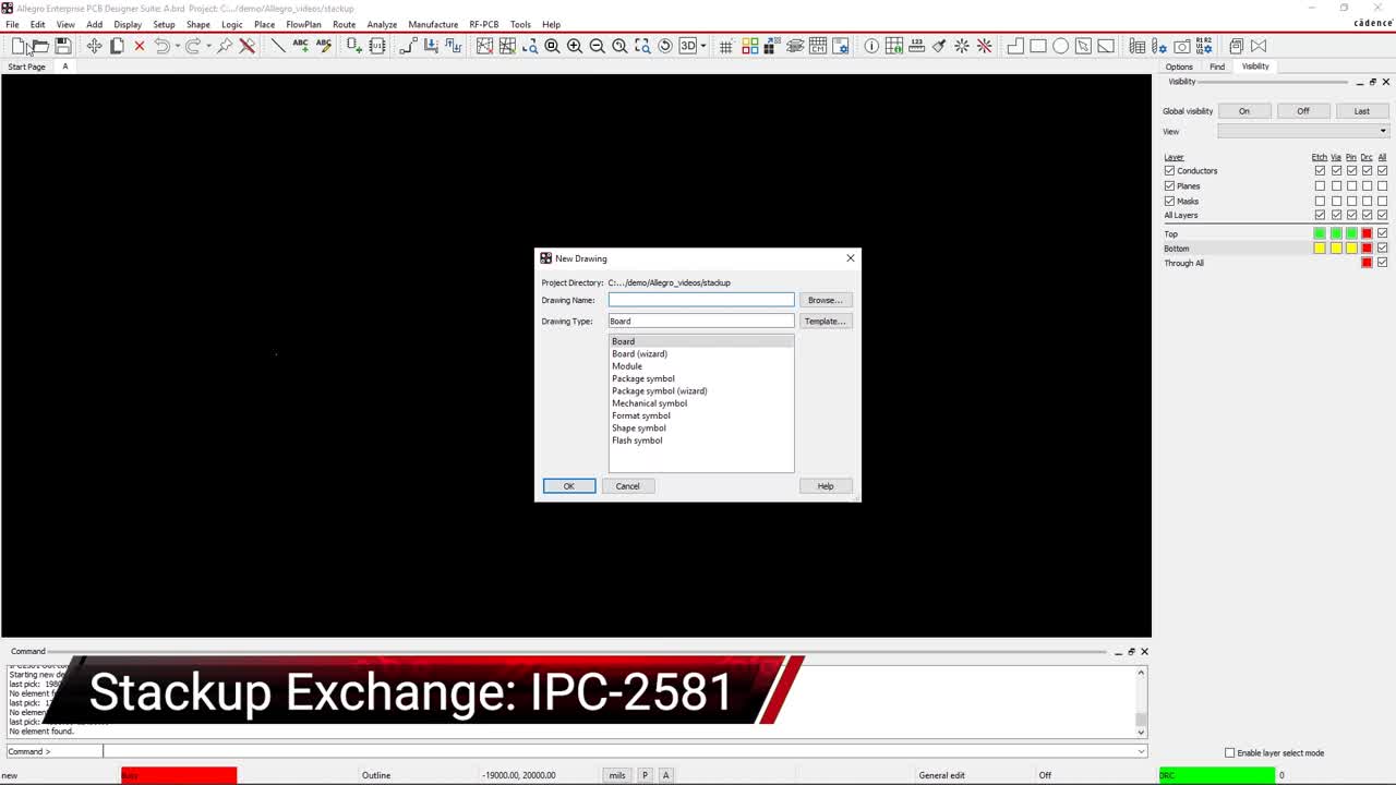
Lastly, being able to merge the tools with the industrial knowledge of the contract manufacturers would be the best of both worlds. Here is where EDA vendors like Cadence have made real strides with the Allegro PCB Designer system. Allegro provides the capabilities for designers to communicate bi-directionally with participating manufacturers in order to exchange board layer stackup information through the IPC-2581 format. Designers can receive board layer stackup information directly from the CM and then send them fabrication and assembly data for manufacturing.
Using the Stackup Creation Utilities in Your PCB Tools
To show how this can be done, let’s take a look at the capabilities of Cadence Allegro in the creation of a board layer stackup. Allegro is a full-featured design tool that can take your design from schematic all the way through layout. In the picture above, you can see the six-layer board stackup that was generated automatically using the Allegro board creation wizard. Notice that the values are all generic with a couple of the pull-down menus displayed to show the board dielectric material options that are available for the designer to choose from.
In the picture below, the layer stackup has been fully completed. Additional layers have been added, including silkscreen, solder paste, and solder mask. Also, layer names, functions, and widths have been added, as well as fine-tuning for the board materials and dielectric constants. Now that these layers have been fully defined, they are properly configured to work with the rest of the functionality in Allegro PCB Designer to calculate controlled impedance routing and other design data.
The Cross-Section Editor in Cadence Allegro
With advanced PCB design tools like Cadence Allegro, you will have the capabilities that you need to fully setup and configure your design for layout. To read more about this process, take a look at this E-book.
If you’re looking to learn more about how Cadence has the solution for you, talk to us and our team of experts.