Balancing Multilayer Circuits with Plated Holes: Placement and Information
Key Takeaways
-
Learn about circuit board holes and how they are made and used in PCB design.
-
Routing tips that can help manage the placement of holes.
-
How to use the features within your PCB design tools to help.
Since a hole is the absence of material, it is only natural to think of a hole as being empty and, therefore, not taking up any space. But, we know that isn’t true; a hole can actually take up a lot of room in the overall landscape. Just consider the Grand Canyon, which is one of the biggest holes in the world. At 277 miles long, up to 18 miles wide, and over a mile deep in some places, it takes up plenty of space, as anyone who has driven in that area can attest to.
The holes in a circuit board also take up a lot of room, and if we aren’t careful about where we place them, we can find ourselves running out of space very quickly. Holes are obviously important for component thru-pins and routing circuitry between board layers, but they can also cause problems if not placed correctly. Here are some of the problems that can come up when designing multilayer circuits with plated holes and how you can successfully work with them.
The Different Types of Holes Used in PCB Design
A printed circuit board can have a variety of different holes for a number of different purposes, and together, these holes will take up a lot of room. These holes can be separated into three classifications: mechanical, component, and vias:
Mechanical Holes
Circuit boards will often have holes in them for manufacturing purposes, and these are known as “tooling” holes. They will enable the manufacturer to hold the board in place for fabrication and assembly. There are also holes used for mounting the circuit board to other objects such as the chassis of the system. Mounting holes may additionally be used for installing non-electrical objects onto the board such as brackets, shields, or ejector levers. In some cases, these holes may be plated with metal but most of the time they are not and are referred to as non-plated thru-holes, or NPTHs.
Component Holes
While the majority of electronic components in use today are surface-mount packages, there are still some components that require thru-hole technology. These include connectors, switches, and other interface parts that require a more durable mounting to the board and high-current components that need a more robust solder connection. Some surface mount components will have their own built-in mounting holes for durability, grounding, or thermal relief.
For these components, a plated thru-hole, or PTH, is required. These holes are mechanically drilled after the board layers are laminated together during the fabrication process and then plated inside and out with copper. During assembly, the leads of the components are inserted through the holes in the board. The board is then run through wave soldering where the solder will wick up into the holes and around the leads forming a solid solder connection.
Via Holes
Vias conduct signals, power, and ground through the layers of the board. There are different types of vias that can be used depending on the needs of the circuit board layout:
-
Thru-hole: These holes are fabricated the same way as a PTH component hole but are generally smaller in size and can go down to 0.006 inches in diameter.
-
Blind: For vias that are not desired to go all the way through the board, these holes are started on either the top or bottom layer of the board and then only drilled partway through. This frees up more room for routing beneath them but they cost more to fabricate than a standard PTH via.
-
Buried: A buried via only goes part way through the board layers, as a blind via does, but it starts and stops on internal layers only. This can be very helpful in circuit boards with multiple layers, but it also adds additional fabrication costs.
-
Micro: For holes that need to be smaller than 0.006 inches, a microvia will be used. These vias are laser drilled and typically only span two layers of the board. Due to their smaller size, it is very difficult to plate the holes beyond two layers of depth. Micro vias can be used in a variety of ways including stacking them together or with blind and buried vias, but they have a higher fabrication cost as well.
As you can see, there are many different hole types that can be used in a circuit board. Although thru-hole components are still regularly used in PCB design, the majority of the holes in a circuit board will be for the vias. These vias are critical for trace routing but they take up space and can create performance problems if not used correctly in multilayer circuit boards.
Next, we’ll look at ways to balance the needs of vias and multilayer circuits in order to correctly design the board.
Vias in a circuit board.
Escape Routing Fine-Pitch Devices
One area of the board that will quickly get filled up with vias is around the high pin count parts, especially ball grid array (BGA) components. With hundreds or even thousands of pins needing to be routed out of these devices into the board, the space on the PCB will get used up very quickly. In order to route out of the devices successfully, it is important to develop a strategy for these escape routes. Here are some ideas to keep in mind that can help:
-
Plan your component placement around these parts with the routing in mind, starting first with the decoupling capacitors. High pin count parts rely on many capacitors to balance their power integrity and there won’t be enough room for them after the routing has been completed. From there, place the remaining components that the device will connect to according to their signal paths. You also need to maintain enough room for routing channels and vias when placing all of these parts.
-
Plan the escape via placement carefully allowing for enough routing channels beneath the part. Usually, this starts by routing the outer rows of pins first in diagonal patterns away from the part. Next, route out from the pins to vias that are directly next to them in a dog-bone pattern or route the pins inward if your BGA has an empty area at the center.
-
For larger BGAs, use vias within the BGA pads to conserve space. It is important to check first with your manufacturer to ensure that they can assemble the board with vias in pads. For BGAs with higher pin counts and/or smaller pin pitches, you will want to use microvias and/or microvias in pads.
With so many nets to route out of these high pin count devices, there is no way to avoid having a lot of holes in the board in these locations. The key is to plan out the design before you start placing parts and routing them so that you have the room you need to get everything in. Next, we’ll look at how the location of vias can affect the routing across the rest of the circuit board.
A row of larger holes in a circuit board that has clogged up a path for return signals on a reference plane.
Routing Multilayer Circuits with Plated Holes
After routing out of dense BGA and other high pin count packages, it would seem like most of the problems with balancing multilayer circuits with plated holes would be over. But, there are other areas of the design that can still sneak up and cause problems if you aren’t careful with how you locate the holes in the board. Take the return paths of the high-speed sensitive signals for instance.
If a high-speed transmission signal isn’t able to cleanly return to its source through the reference plane, it can potentially create electromagnetic interference in the board. This can lead to a degradation of the board’s signal integrity which will decrease the performance of the circuitry or even shut it down. As you can see in the picture above, the placement of vias in this high-density routing area of the board has choked off that spot in the reference plane for clear signal return paths. This will force a signal to wander around the board in an attempt to return to its source, creating noise along the way.
To avoid problems like these, here are some layout steps that can help:
-
Be careful when planning split planes to provide power in high-density routing areas. These splits are often responsible for choking the signal return paths.
-
Set up net classes in the PCB design CAD system to control what via types are used for different groups of nets.
-
Use the design rules and constraints to check for how close vias are to each other to make sure that you don’t inadvertently block routing channels or return paths.
-
For signals that have to transition from one layer to another using a via, consider using a ground transfer via next to it. This will maintain the return path on the reference plane along with the signal.
There are a lot of considerations to keep in mind when using vias in the routing of your printed circuit board, and these are just a few of them. To keep all of the layout and manufacturing needs of your PCB organized, it is important to use the full capabilities of your design tools, which is what we will look at next.
The constraint manager in Allegro PCB Editor showing same net clearances.
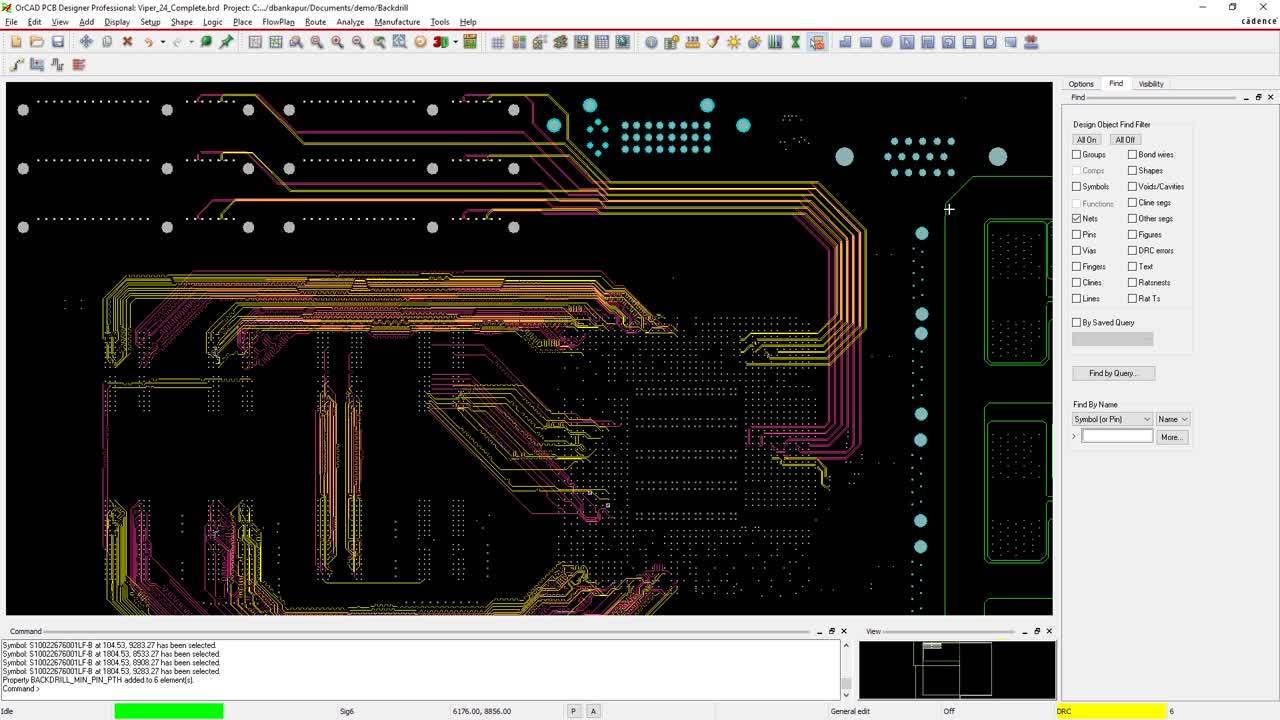
Putting Your PCB Design CAD Tools to Work
Your PCB design CAD system will have a lot of tools that can help you to balance the plated holes in your multilayer circuits. You can usually find schematic capture tools that integrate with the layout tools, circuit simulators, and signal and power integrity tools as well. Within those tools are many features that can help, such as design rules that can be set up across both the schematic and layout environments to create net groups for via assignments.
In the case of Cadence Allegro, you have a complete constraint management system that allows for multiple rules to be set. In the picture above you can see the settings for some net clearances in the constraint manager. Rules and constraints like these can help you to control where your vias are placed in the design in order to balance the holes with the circuitry.
There is a whole lot more to working with plated holes in PCB designs than what we’ve covered here. For more information on this subject, take a look at this E-book from Cadence.
If you’re looking to learn more about how Cadence has the solution for you, talk to us and our team of experts.