Layout Best Practices for PCB Board-to-Board Connectors
Key Takeaways
-
Board-to-board connectors; their types and usage
-
Layout guidelines for board-to-board connectors
-
PCB design tool features that can help when working with connectors
A header connector on the edge of this circuit board
One of the advantages of building an electronic system with separate printed circuit boards is that it makes repairs or enhancements easy due to its modular approach. This is especially common with computers where memory is routinely added or defective graphics cards are replaced. Simply swap out the older board with a new one, and you are back in business. The reason that this process works so well is that circuit boards are typically designed with board-to-board connectors that make replacing the PCBs easy.
The connectors that join circuit boards together in an electronics system are typically not complex. However, there are some differences between them, depending on their application, and it is important to follow some basic rules when placing them in a layout. To fully understand the requirements of working with PCB board-to-board connectors, let’s take a closer look at what they are and how to use them in your next layout.
Interconnecting Circuit Boards With Connectors
Board-to-board connectors, or “headers,” give PCBs the ability to be connected together without the use of wires or a harness. One board will have a connector with pins, while the other board will have the mating receptacle. While variants of these connectors can be used with wiring harnesses, their main benefit of a board-to-board header is providing a short and direct connection between the two circuit boards.
Board-to-board connectors are available in many different forms, depending on the needs of the PCBs they are connecting. They come in different packages, mounting styles, and pin pitches. For circuit boards with taller components, a designer can choose a correspondingly taller connector. The application that the connector will be used for also needs to be contemplated. Designers need to consider the current that the connector will be conducting and choose a header that can sustain that level without damage. Next, we’ll look more into the different variants of these connectors that are available to you.
Headers like this are used for board-to-board connections
Different Types of PCB Board-to-Board Connectors
We’ve already mentioned the differences in height and package styles that PCB board-to-board connectors are available in, but there are other differences as well. Here are the four main areas of connectors to be aware of when choosing between them.
Types
A board-to-board connector’s type is based on its plastic base that contains the contact pins. The connectors are either plugs, receptacles, or, as they are more traditionally referred to, male and female headers. The headers may be configured with straight pins or with pins bent over at 90 degrees for a right-angle connector. These connectors can be stacked to elevate them on circuit boards that have taller components and require more clearance between boards. When the connectors are shrouded in plastic, they are known as box headers and are typically used with ribbon cables. These headers are polarized by a raised surface on one connector that matches the notch in its mating header.
Technology
Board-to-board connectors are available in both thru-hole and surface mount pin configurations. Thru-hole pins provide a much more robust physical connection and are useful for connectors that will constantly be plugged and unplugged throughout the life cycle of the board. The connector pin pitches are also available in standard hole spacings, making them very useful for breadboards, or at other values as well. Surface mount connectors, on the other hand, can be much smaller, which takes less room on the board and costs less. However, they do not have the same mechanical stability as a thru-hole connector, which can cause problems for some boards, especially those that are under a lot of physical stress.
Contacts
The pins used in board-to-board connectors are available in different plating options including copper, gold, nickel, and silver. Headers are also available with more rows of pins, depending on how many nets need to be connected. It is also important to consider the amount of current that the connector will be carrying and choose a connector with the appropriate rating. Lastly, while smaller pin-pitches will allow you to increase the connector pin-counts, they can also cause a problem with routing traces on the board. You need to make your connector choices considering the routing density of the board as well.
Features
Board-to-board connectors are also available with unique features specifically designed for special case manufacturing or operating environment needs of the circuit board as well. For example, some headers are built to be “press-fit” and do not require soldering. Other connectors are designed to be hermetically sealed or resistant to chemicals, and others are configured with filters to block EMI. Some headers are also equipped with locking mechanisms to prevent inadvertent disconnects.
Once you’ve selected the best board-to-board connector for your design, the next step will be incorporating the header into your PCB layout.
PCB layout design rules like these can be used to set clearances around board-to-board connectors
PCB Layout Strategies and Concerns When Designing With Connectors
The needs of the circuit board configurations within the system will dictate how the headers will be placed on each individual board. Here are some possibilities to consider:
-
Boards that need to be parallel with each other will be stacked using straight pin headers.
-
Boards that need to be side-by-side horizontally will be connected with right-angle headers.
-
Boards that need to be positioned at right angles to each other will use a combination of a straight pin header on one board and a right angle mating connector on the other.
When placing the headers, be sure to allow enough clearance around them for the mating connector to seat properly without obstructions. Your PCB design tools will have design rule checks for component-to-component spacing, as you can see in the picture above, and you should ensure that they are set up properly for the headers that you are using. Consider the test and debug needs of the PCB as well, and allow enough clearance near the headers for technicians to work on the board. Also, look for unexpected obstructions that might not be reflected in the library parts. Heat sinks, brackets, and other board objects can end up getting in the way if you aren’t careful.
Another area that you should be very careful about is the pin-outs of the connectors. The first step is to ensure that the pin-outs in the connector footprint are what you were executing based on the schematic symbol used for the header. Secondly, check and double-check that the mating connectors on both boards have pin-outs that match each other. Ensuring that your silkscreen has pin number markings on it can help quite a bit with this checking. There are some other features in your PCB design tools that can help as well, and we’ll look at those next.
The 3D checking in Cadence Allegro shows a collision between the header and another component
Design Tool Features to Augment Connector Placement and Routing
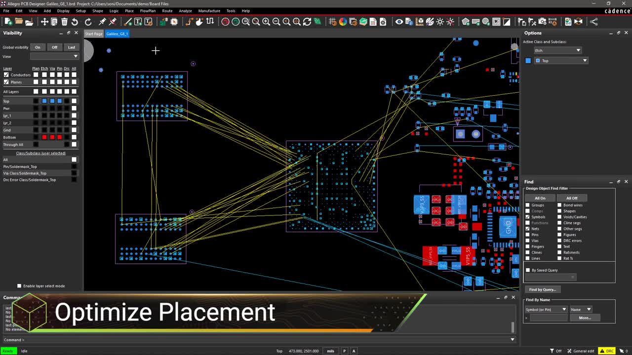
The PCB design tools that you are using will have many more features in them to help with placing board-to-board connectors than just the regular design rule checks. One of the first features that you should use is the library tools and plugins that are available to you. These will check your parts to ensure that you are using the latest versions and connect you with online component suppliers for symbols, footprints, images, and other part information that can help you with your design.
Another very useful feature is the 3D viewing capabilities of your design tools. In the picture above, you can see how the Cadence Allegro PCB Editor is displaying the layout in 3D. In addition, it is doing a DRC of the 3D layout and showing an error condition where another part is in conflict with the connector. The ability to work with 3D tools in your circuit board layout can give you a much-needed perspective on how the parts will really look in relation to the rest of the board.
Finally, pulling in mechanical data as well as other system layouts will help you to design your PCB board-to-board connectors knowing how they will plug and play with the rest of the PCBs in the system. This will give you the ability to find potential obstructions and conflicts before you have a prototype built and save you time and money on multiple board spins during product development.
For more information on how ECAD design can work with MCAD design, check out our E-book on the subject.
Leading electronics providers rely on Cadence products to optimize power, space, and energy needs for a wide variety of market applications. To learn more about our innovative solutions, subscribe to our newsletter or our YouTube channel.