Optimizing PCB Design Rules for Digital Circuits
Key Takeaways
-
The electrical and manufacturing requirements of digital circuits.
-
Setting up design rules for component placement, routing, and metal planes.
-
Additional uses of advanced PCB design rules for digital circuits.
Closely placed components on a circuit board
Anyone who has laid out a printed circuit board is undoubtedly familiar with PCB design rules and constraints. Introduced early on in the development of PCB design CAD tools, rules and constraints initially kept the designer from shorting different nets together, but that was about it. While this was a tremendous help at the time, PCB designers continued to ask for more functionality in their design rules to cover the different types of circuitry configurations they were working with.
In today’s CAD systems, design rules and constraints have been enhanced to give designers the type of control they need. This has been a welcome relief, as designers often find themselves working with complex designs that incorporate power, analog, RF, and digital circuitry all on the same board. In this article, we will explore some of the requirements associated with PCB design rules for digital circuits and how you can best optimize these rules for your next layout.
Electrical and Manufacturing Requirements of Digital Circuits
For a circuit board to operate electrically and to be manufactured without errors, it must be designed according to a specific set of rules. Not only do these rules govern the size and shape of different elements on the circuit board, but they also enforce spacing between the elements. The elements that are governed by these design rules can include components, traces that connect the nets between components, and vias that interconnect the traces between different layers of the board.
Component Placement
The parts on a circuit board need to be placed strategically to provide the best connection lengths between them. This becomes especially true when working with high-speed designs, where several components may be part of an entire high-speed signal path. Other components, such as bypass capacitors, need to be placed close to the power pin on the devices they are assigned to and power supply components need to be as close as possible to each other.
As close as those placement requirements are to each other, the parts still need to be positioned to best facilitate PCB manufacturing. Circuit board components need to have enough clearance between them for automated assembly, soldering processes, and manual rework. Connectors and other human interfaces require accessibility and parts must also be located with thermal cooling kept in mind.
Trace Routing
Differential pair routing on a printed circuit board
While a good percentage of a circuit board’s trace routing can be handled with default values, many nets will require unique trace width and spacing values, including the following:
- Differential pair routing: Differential signaling requires two identical signals, with one being inverted, to transmit one complete data signal. The signal's information is deciphered from the difference between the inverted and non-inverted signals. This reduces noise and EMI but requires the two signal traces to be equal in length with consistent widths and spacing (as shown in the picture above).
- Clock and data lines: Clock signals coordinate the activity of the circuitry and their pulses will trigger the inputs and outputs of data. This requires adequate spacing between these sensitive lines and other signals as well as specific trace lengths to ensure that the clock and data lines match each other.
- Impedance controlled routing: Capacitance and inductance in high-frequency traces create an opposition to the current flow of the signal and can degrade the signal’s quality. Controlling this requires specific layer thicknesses and dielectric materials in the board stackup, precise trace width and thicknesses, and close proximity to the signal’s return path on the adjacent reference plane layer.
Vias
Different sizes and shapes of vias are used depending on the nets they are used in. For instance, power and ground nets will usually require larger vias than regular signal nets. Vias can also vary in type, with high-speed routing using smaller blind and buried vias or micro vias for both physical space and electrical performance.
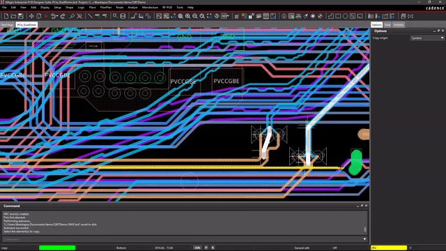
These different electrical and manufacturing requirements can be controlled by design rules set up in PCB layout tools (as shown in the picture below). However, there are still more requirements that need to be considered for a design.
An example of how differential pair routing can be set up in the PCB design rules for digital circuits
Power, Ground, and Reference Planes
Power and ground traces can end up having several different trace width and spacing values depending on the requirements of the circuitry. Routing traces within power supplies on a digital board, for instance, can call for unusually wide traces to handle the increased current and temperatures. The wide traces will also help the power integrity of the board by reducing inductances and controlling the noise of crosstalk.
While there will be short connecting traces that must be width and spacing controlled, most of the power on a multi-layer circuit board will be conducted through copper pours and metal plane layers. These also must be controlled to ensure that your power delivery network (PDN) is providing clean power to all of the necessary components. Fortunately, these power routing widths and plane connections can all be controlled through design rules (as shown below).
Setting up rules and constraints for power and ground on a PCB design
Another important part of the PDN is the ground planes in the board layer stackup. These layers are critical to the signal and power integrity of the board and provide the following benefits:
- Clear return paths: To eliminate the chance of noise being created by wandering signal returns, a ground reference plane offers a clear and direct return path for high-speed signals.
- EMI shielding: Ground planes also provide shielding to protect sensitive circuits from the threat of external electromagnetic interference.
- Filtering switching noise: As digital circuits switch between high and low states, they can create another source of noise in the ground circuit. By using a large metal plane, the noise will be reduced by the lower impedance of the plane as opposed to routing ground with a trace.
- Heat dissipation: Ground planes also help dissipate the heat of hot-running components by serving as a heatsink.
Another important part of both power and ground planes is controlling the connections with thermal relief pads. These spoke-shaped elements prevent the large metal plane from acting as a heatsink for soldering efforts while still providing enough of a connection for good power integrity.
All of these components, routing, via, and plane considerations have to be controlled through the use of PCB design rules. Next, we’ll look at how these rules can be set up and optimized for the maximum benefit to your design.
Setting Up PCB Design Rules for Digital Circuits
Most PCB design CAD systems in use today have the capability to transfer rules between the schematic and the layout. This is a huge benefit for the design team, as it allows the schematic to drive design rules instead of waiting to input all the constraints on the layout side. This level of organization gives electrical engineers the ability to set up specific net and component rules that are essential for the circuits they are designing. The layout team also doesn’t need to rely on written or relayed instructions, as the net rules are already present in the design database.
Here are the areas of PCB design rules for digital circuits that should be focused on to ensure the circuit board is laid out correctly:
-
Default values: Most design tools will start off with a set of default values in their design rules. These can be “left-overs” from previous designs or true system defaults. It is incumbent on the layout designer to confirm these values before they start to ensure that they aren’t routing with incorrect trace widths or placing components too close to each other.
-
Classes: While most design rules can be set up for individual nets or components, this can be very tedious to work with if you have hundreds of objects that require unique rules and constraints. Most design tools offer a system of setting up classes of nets and components to make rules and constraints set up easier. For instance, you can set up unique trace width and spacing requirements for the +5V, -5V, +15V, -15V, and 3.3V nets, or you can create a set of rules for one power class and add those nets to it. The same goes for classes for clock and data nets and different types of components.
-
High-speed design rules: Design rules are also available for high-speed constraints, and layout teams should use the full capabilities of their design rules for maximum benefit. For instance, specific trace lengths can be set up as well as length matching to other traces, which is very helpful when routing clocks and data lines. Differential pairs can be set up to route the traces together at set distances from each other and unique trace topologies can be specified for specific net characteristics. Trace widths can also be set automatically for impedance-controlled routing and via types and sizes can be specifically assigned to nets or net classes.
There are many different design rule features in a modern PCB design CAD system for digital circuits; we’ve only covered the routing constraints so far. Next, we’ll look at some of the other rules and constraints that can be set up.
Design for assembly rules in the Cadence Allegro Constraint Manager
Additional Uses for PCB Design Rules and Constraints
In addition to the standard PCB design rules for digital circuits—including component placement, trace routing, and power and ground—there are a number of rules that can be set up specifically for manufacturing. Among those are rules governing solder mask webbing, solder paste coverage, silkscreen overlap, and test point spacing. PCB design CAD tools such as Cadence’s Allegro PCB Editor have specific rule sets for circuit board fabrication and assembly that contain these and many other rules as well. You can see an example of those assembly constraints in the image above.
Design rules and constraints are also used when importing data from mechanical CAD systems to check object-to-object clearances between the board and the system enclosures. Many systems, such as Cadence Allegro, have full 3D canvas capabilities that allow users to both view and check their designs to the imported mechanical data or even to other PCB designs. And, once design rules have been fully set up and refined, they can be exported and saved for use in a future design.
To find out more about some of the advanced capabilities of PCB design rules and constraints when working with ECAD and MCAD data, check out this E-book.
If you’re looking to learn more about how Cadence has the solution for you, talk to our team of experts.