PCB Component Orientation Considerations for Optimum Part Placement
Key Takeaways
-
PCB footprint considerations that can affect component placement
-
Electrical and manufacturability concerns with PCB component orientation
-
Using your PCB design tools to help while you are placing parts
Color-coded visual cues help provide placement guidance against certain timing constraint values.
Have you ever found yourself driving the wrong way down a one-way road? There’s nothing quite like that shock of fear and embarrassment when you suddenly realize your mistake. Heading in the wrong direction like that can certainly cause difficulties for you and your car, just as pointing components in the wrong direction can create problems in your PCB design. No, the parts won’t end up crunched in a traffic accident, but their orientation can impact both the electrical performance and the board’s manufacturability.
At one time, the slower circuitry of older circuit boards allowed PCB designers a lot more latitude in how they placed their components. If a longer trace was needed to route the part, it wasn’t a big concern. With the faster signal speeds, power integrity concerns, and thermal considerations in today’s designs, that luxury is now gone. Layout teams must consider the needs of both electrical performance and manufacturability when deciding on the PCB component orientation of their designs. Here is a closer examination of why this is so essential.
PCB Library Considerations for Placing Components
The correct orientation of a component on a circuit board starts with how the component footprint is constructed. If the part has been built incorrectly, even the correct component orientation will still result in a miss-connected part. It is very easy to swap the two pins around on polarized parts, and diodes will often get their cathodes and anodes misinterpreted too. Sometimes, parts with multiple pins will be built with pin one in the wrong location or their numbering sequences all out of order.
To guard against these problems, it is always best to have the latest datasheets and part information on hand when building PCB component footprints. Another useful tool to use is the part building wizards and utilities in the design tools you are using. Many tools today also have connections to online library services that will allow you to download part information including schematic symbols, PCB footprints, 3D step models, and more. With these services, you can save yourself a lot of time that would normally be devoted to library work. Another benefit is that most of these models come directly from the component manufacturers, guaranteeing that the parts you are using in your design will be correct.
There are also some things that you can do with your component footprints that will help with parts placement in the layout. If you can, place markers in your footprints for the component’s polarity and pin one location. This will help later on in layout to place the part in the correct orientation, which is essential for the board’s best electrical performance, as we will see next.
Using an external library browser to download symbols, footprints, datasheets, and images into a design
PCB Component Orientation and Its Effect on Electrical Performance
At one time, a circuit board could be laid out with its parts arranged aesthetically and it would perform just as well. However, that is no longer the case—today, PCB components must be placed in specific partitions according to their function for optimum performance. They also have to be oriented correctly to satisfy the needs of the signal or power circuitry they are servicing.
High-Speed Signals
There is more to a high-speed circuit than just a single point-to-point connection. High-speed circuitry often consists of multiple nets that together make up one complete signal path. For instance, a signal path may start at a source and then go through a resistor before terminating at its load. Therefore, the signal path consists of two nets with a resistor in the middle, and for the best signal integrity, both nets need to be treated together as one. To accomplish this, the resistor must be oriented to provide the most optimum connection between the signal path’s two nets.
High-speed routing also consists of memory and data buses that contain many nets. Not only do these nets need room for their trace routing, but for escape vias as well. This requires that all components connected to these nets be orientated in the most optimum direction for the shortest possible trace routing. In the same way, components that are part of impedance controlled nets must be oriented for the shortest and most direct connections, especially those that need to be routed with differential pairs.
Power Supplies
Power supply components must also be oriented for the most optimum connection configuration during placement. To reduce the inductance and resistance as well as the noise that can be created in high current power supply traces, the routing must be as short and as direct as possible. This will require a very tight placement of the power supply parts and possibly some unusual component orientations. Additionally, power supply components should also all be placed on the same side of the board to help with the short and direct routing.
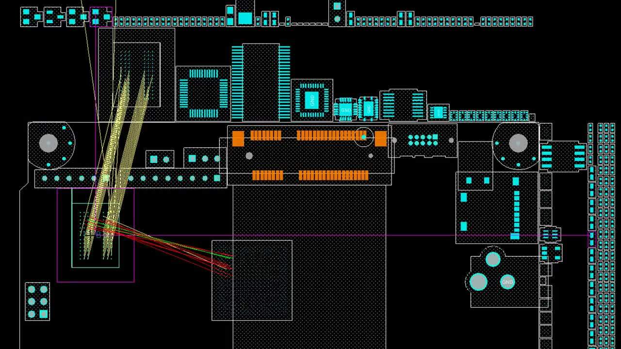
Satisfying all of these signal and power integrity needs will require some creative placement of the PCB components. Some of these parts may end up having to be orientated at odd angles instead of the usual 90-degree increments to achieve the best signal and power routing. The key is to check first with your manufacturer to see what they can and can’t build before starting your board placement.
Components placed at different orientations to keep trace routing as short as possible
Manufacturability and PCB Component Orientation
The goal of design for manufacturability (DFM) rules is to make PCB manufacturing more efficient. This will reduce errors and time, which, in turn, will cut expenses. Some companies put tight restrictions on their board designs to keep all the passive components oriented in the same direction. This minimizes the amount of time required to rotate these smaller parts during assembly. While this may seem like a minor issue, it can add up when building thousands of boards, each with hundreds of these passive components on them. Here are some other basic manufacturing rules about component orientation that designers should keep in mind.
Automated Assembly
-
Wave soldering: Be careful to orient smaller two-pin components perpendicular to the board’s direction going through the wave. This way, the two pins will be soldered equally. Also, be careful about locating taller components where they will proceed smaller parts into the wave. The taller components may shadow the smaller ones and prevent them from being completely soldered.
-
Solder reflow: The main concern in reflow soldering is how the part is heated. If a two-pin component is heated unequally due to excessive metal connected to one of the pins, the part may pull towards the other side as it melts quicker. This can cause the component to stand up on one end in a manufacturing error known as “tombstoning.” To avoid this, the part should be oriented differently, or the metal connections equalized between the two pins.
Rework and Test
Technicians need access to the parts on the board to debug and rework them if necessary. If the components are not oriented optimally or are placed where they are difficult to get to, this also can add time and expense to PCB manufacturing. In the same way, automated testing will require specific clearances between test points and components and the edge of the board for the test fixture. Components may need to be rotated to make more room for this.
There are a lot of requirements to remember when considering component orientation in a PCB layout. Fortunately, your design tools can help with a lot of this, and we will look at that next.
Setting up the clearance rules for component placement in Cadence’s Allegro PCB Editor
Using Your PCB Design CAD Tools to Help With Component Placement
There are a lot of different features and utilities built into CAD tools that can help with PCB component orientation, such as the online library service tools we looked at earlier. Simply changing net colors or other layout parameters can also help to simplify the component placement. For parts that require fixed orientations on the board, look into restricting their ability to be rotated while you are placing them. This is something that can usually be set up with different tool parameters.
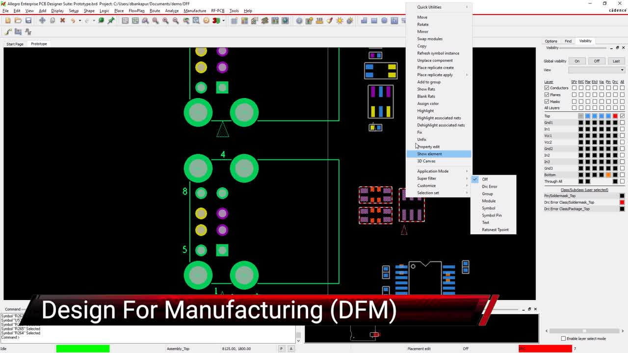
It is also important to use your design rules and constraints as much as possible. With these rules completely set up, you will get online warnings from your CAD system if you place a part that is in clearance violation to another. The picture above shows how the placement rules are being set up for a layout in Cadence’s Allegro PCB Editor. These same rules also get used when viewing the board in 3D to check the clearances to other mechanical objects in the design.
To find out more about how you can avoid some of the more common design for manufacturability (DFM) rules during PCB layout, check out the information we have for you in this E-book.
If you’re looking to learn more about how Cadence has the solution for you, talk to us and our team of experts.