PCB Thermal Relief Guidelines for Effective Layouts
Key Takeaways
-
What are thermal relief pads in PCB layout?
-
Guidelines for creating thermal relief pads.
-
How to use your PCB CAD tools when creating thermal relief pads.
PCB thermal relief guidelines are used in creating these pads to aid in manufacturability
A thermal relief on a circuit board ensures that the proper amount of heat is focused on a pin for soldering. Without thermal reliefs on circuit boards, there would be a wide range of assembly problems associated with soldering. Some pins wouldn’t get enough heat for the solder to form a proper joint, and other parts would be difficult for technicians to unsolder during rework. Inversely, this could turn the relief into an unplanned fuse. It is essential for layout engineers to understand good PCB thermal relief guidelines when setting up the CAD system parameters of their design to avoid thermal problems.
The Importance of Thermal Reliefs in PCB Layout
Thermal reliefs are the spoked connections from a thru-hole or surface mount pad to an area fill or plane. Their purpose is to provide a robust electrical connection from the pad to the plane while preventing the heat needed for soldering from dissipating into the metal plane. The green color represents a solid plane of copper on a circuit board in the picture below, and you can see four thermal relief connections for each outer pin. In the case of a surface-mount pin that connects to a large metal area, multiple traces may be used from the pad to the copper to accomplish the same results.
The purpose of the thermal relief is to aid in the manufacturability of the circuit board. While a direct flooded connection gives the best electrical performance, it also serves as a heat sink for pins connected to the plane. This sink could effectively pull the heat away from the pin during automated soldering operations and produce poor solder joints in the connection. Simultaneously, the heat sinking attributes of a direct connection would make manual soldering operations difficult for technicians during rework. Additionally, too much metal on one pad versus the other on small two-pin discrete parts can cause a thermal imbalance in the component. This imbalance can result in a manufacturing phenomenon known as “tombstoning.”
However, it is also imperative that the spokes of thermal reliefs be thick enough to handle the current expected to pass through them. Balancing the number and widths of thermal relief spokes is crucial for a good thermal relief design. Spokes that are too small may not conduct enough current for power circuits or provide inadequate connections for power integrity. Spokes that are too large may end up drawing too much heat away from the pad. Again, in the picture below, you can see how wide the spokes of these thermal relief pads are to provide the correct amount of copper to connect the pin to the plane. Next, we’ll look closer at the guidelines of where and how designers should use these reliefs in PCB layout.
Standard thru-hole pin thermal relief pads
PCB Thermal Relief Guidelines for Layout
The need for a thermal relief pad can come up during different aspects of PCB layout, and here are four areas where designers should consider their use.
1. Thru-Hole Pins
Holes drilled through the board for soldering of thru-hole pins are prime candidates for thermal relief pads. A small metal area, such as a split plane, can act as a heat sink and pull heat away from the pin. In large multi-layer boards with multiple ground planes, the thru-hole pins may be connected to several square feet of metal, requiring an excessive amount of heat to create a good solder joint. This heat requirement opens up the possibility of nearby traces and components being damaged when applying extra heat during soldering operations. Thru-hole pins like these need a thermal relief pad to provide a good electrical connection without the heat sinking characteristics of a direct connection.
2. Surface Mount Pins
For electrical reasons, many designers will embed a surface mount pad in a metal fill. While this will give the best electrical performance, it also pulls heat away from that pad. If these pads belong to a small two-pin discrete part, the solder on the other pad may melt faster than the embedded pad. The resulting surface tension of the melting solder will pull the part up and away from the other pad, creating a tombstone. By using multiple traces to connect a surface mount pad instead of embedding it into an area of metal, you can balance the amount of heat applied during soldering between both pads.
3. Vias
Most vias that connect to power and ground do not require a thermal relief pad because they don’t have a pin soldered into them. However, in the case of nets that conduct high current levels, some short power traces may still conduct too much heat to their surface mount pins. In these cases, a thermal relief pin should be considered.
4. Metal Routing
While a thermal relief pad is necessary for pins connecting to power and ground planes or large area fills, their use on power trace routing must be considered for each case. Some power traces that conduct lower levels of current will be routed with narrower traces. CAD systems that automatically add a thermal relief connection to pins on these nets may end up doing a disservice to the design by trying to force the relief pad. The spokes may not have enough room to connect, resulting in a connection without enough metal.
Remember that the number and widths of the thermal relief pad spokes should equal the width of the trace dictated by its power requirements. If you are routing a 50 mil power trace, but you can only get two ten mil spokes to connect, you risk lacking metal for the connection. This lack can lead to excessive heat during the circuit board’s operation, ultimately resulting in a burned-out connection. Additionally, more metal in the connection equals lower net inductance, which will help keep EMI under control. So you must create thermal reliefs with the right amount of metal in their connections, and usually, your PCB CAD tools will have utilities that can help.
Setting up thermal relief pad parameters in Cadence Allegro
Using Your Design Tools to Create Thermal Reliefs
Thermal relief pads are usually created automatically by your PCB CAD system after entering the desired configuration for the pad into the system. When padstacks are built, many CAD systems will allow you to enter the thermal relief’s size, layers, and other parameters into the padstack. Thermal relief parameters can also be configured for each net, plane, or fill in which they will be used. In the picture above, you can see how the user sets up thermal relief attributes for a specific fill in Cadence’s Allegro PCB Editor. The user can set up different parameters for thru-hole pins, surface mount pins, and vias, including how they are connected and how many spokes.
With the thermals adequately configured, they will automatically form when their net is routed with a trace or a fill. In the picture below, you can see an example of how Allegro creates thermals in this simple little copper pour connecting a thru-hole pin to a surface mount pin. The user outlines the desired area, and then the system automatically fills in the copper pour, creating the thermal relief pads as part of the process. The thru-hole pin is connected with two thermal spokes, while the surface mount pin has spokes on all four sides.
Using Cadence Allegro to create a small copper pour and two thermal relief pads
Thermal Management for PCB Layouts
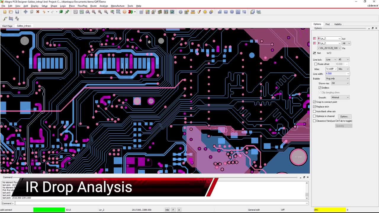
Thermal relief pads are just one aspect of the thermal and other power-related issues to consider and design when laying out a printed circuit board. Fortunately, CAD systems like Allegro’s PCB Editor contain many different utilities and tools that help. For instance, at the top of this article is a video describing how Cadence’s IR Drop Analysis can enable designers to create a stable power delivery network in their design. Allegro also features built-in design rules and constraints to ensure power traces are routed at the necessary widths throughout your board design. Allegro also allows designers to view and check their designs in 3D to handily spot areas on their board with restricted airflow and other thermal cooling problems.
For more information on PCB routing and planes, check out our E-book about it.
Leading electronics providers rely on Cadence products to optimize power, space, and energy needs for a wide variety of market applications. To learn more about our innovative solutions, subscribe to our newsletter or our YouTube channel.