What the Schematic Does Not Show in a Flyback Converter
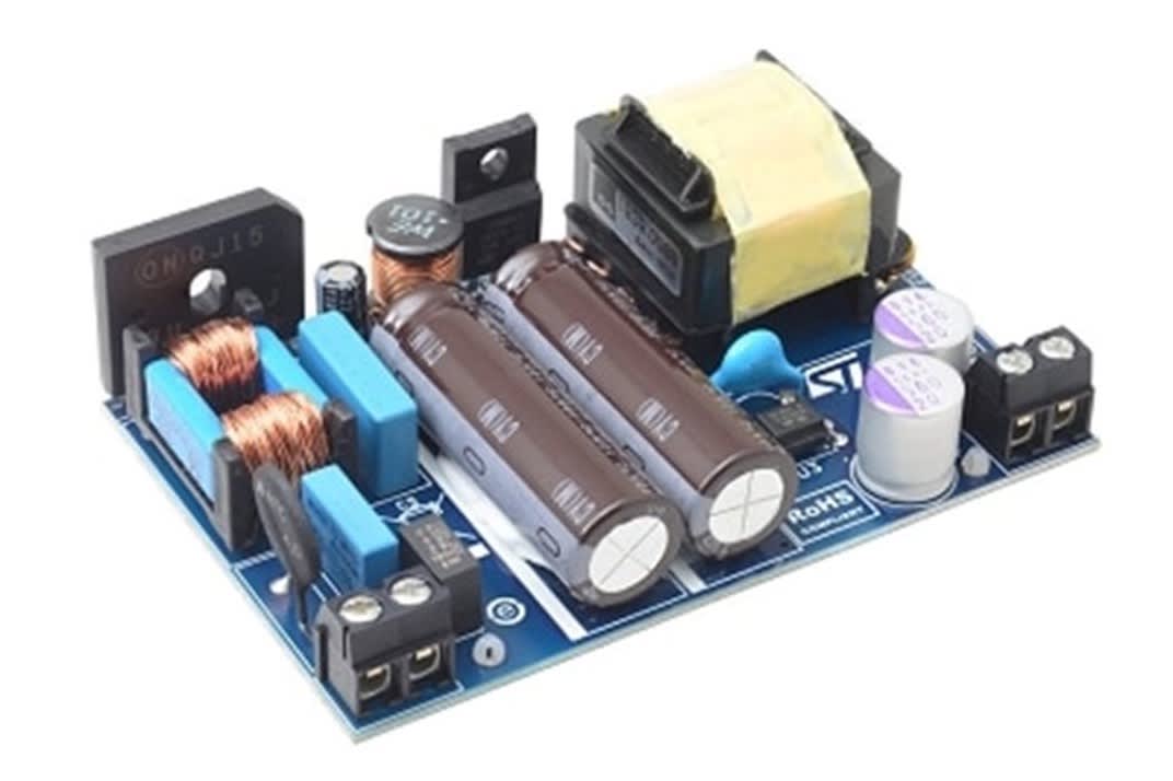
Figure 1. An AC-DC isolated flyback power supply showing the physical separation between primary-side components (input filter, bulk capacitors, and flyback transformer) and the secondary-side output stage. The isolation gap between them is a legal requirement, not a layout preference. (Source: STMicroelectronics)
Flyback is the standard topology for isolated switched mode power supply designs below roughly 100 W. A single transformer provides both galvanic isolation and energy storage. The topology handles wide input voltage ranges without extreme duty cycle swings. Component count is low relative to the isolation it provides.
The schematic looks manageable. That is the problem.
What the schematic does not show is where flyback designs actually fail. Two completely separate ground domains that will break your SPICE simulation if you do not model them correctly. Leakage inductance energy that has nowhere to go at switch turn-off except across your MOSFET. Return current paths on the ground plane that determine whether your design passes a radiated emissions scan. These are not edge cases. They are the predictable failure modes of every first-pass flyback design.
This article covers the decisions that determine whether a flyback design works the first time, and why most of them are invisible in the schematic .
Is Flyback the Right Topology?
Before you commit, confirm the topology fits your application. Figure 2 maps the full selection decision across power converters. The isolation requirement is the first branch point. If you do not need isolation, a buck converter, boost converter, or buck-boost converter will outperform flyback on efficiency and component count at equivalent power levels. Use flyback when isolation is required (whether for an AC-DC converter operating from mains or a DC-DC converter that needs a galvanic barrier), when a wide input voltage range makes non-isolated topologies impractical, or when you need multiple output rails from a single converter.
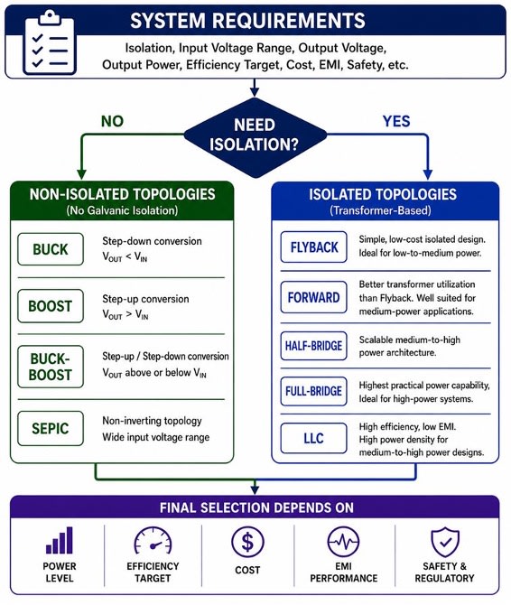
Figure 2. Topology selection begins with the isolation requirement and then narrows based on power level, efficiency target, cost, EMI performance, and safety requirements.
Figure 3 shows where flyback will create challenges once you have confirmed it is the right topology. Read the Typical Considerations column. Lower efficiency at higher power and limited practical power capability are the constraints that define the flyback topology design envelope. Above approximately 100 W, peak switch currents and transformer losses become increasingly difficult to manage. Forward converter and bridge topologies handle higher power requirements better. Know your power budget before you start.
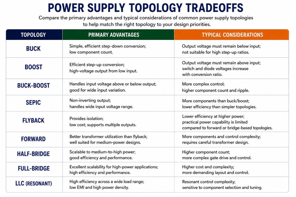
Figure 3. Primary advantages and typical considerations for common power supply topologies. The Typical Considerations column identifies where flyback will create design challenges once the topology is confirmed as appropriate.
What to Resolve Before You Start
These are the questions that need answers before schematic capture begins. Each one drives decisions in flyback converter design that are difficult to reverse once transformer design and PCB layout are underway.
|
Question |
Why It Matters |
|
Is isolation required? |
Determines whether the flyback transformer is a safety barrier, not just a conversion component. If yes, insulation class (reinforced or basic), creepage and clearance distances, and the optocoupler feedback path all become mandatory design requirements. |
|
What is the input source? |
AC mains versus a DC bus changes front-end design, bulk capacitance requirements, and EMI filter strategy. For AC mains, whether power factor correction is required is a mandatory design decision that affects topology and component selection before schematic capture begins. |
|
What is the expected power level? |
Flyback is most practical below 100 W. Above approximately 150 W, power requirements typically favor forward or bridge topologies with better peak current management and transformer utilization. |
|
What operating mode fits? |
Discontinuous conduction mode (DCM) simplifies compensation but increases peak and RMS currents. Continuous conduction mode (CCM) reduces peak currents but the right-half-plane (RHP) zero constrains loop bandwidth. Boundary conduction mode eliminates reverse recovery but runs at variable switching frequency. The choice drives core size, turns ratio, and compensation topology. |
|
How many output rails are needed? |
Multiple secondary windings are achievable but cross-regulation degrades under varying load. Post-regulation may be required for tight tolerances. At higher output currents, evaluate synchronous rectification to recover Schottky diode forward voltage drop losses. |
|
What EMI class applies? |
CISPR 32 Class B for consumer equipment, Class A for industrial. Automotive designs reference CISPR 25. EMI class influences transformer construction, switching power supply PCB design strategy, and input filter design from the start. |
Two Grounds, One Board
This is the part that confuses engineers, and it is the part that is hardest to get right in both layout and simulation.
Your isolated flyback has two completely separate ground references. Primary ground (PGND) sits at the negative terminal of the bulk capacitor, referenced to rectified DC. Secondary ground (SGND) is the output ground. It is the one your load connects to, that users can touch, that may eventually connect to chassis.
These two grounds must never connect on the PCB. The flyback transformer transfers energy across the isolation barrier each switching cycle, enabling DC conversion from input to output. The optocoupler carries voltage regulation signals back across the barrier optically. But galvanically, primary and secondary are completely separate.
In layout, this means two physically separate copper regions with an isolation gap between them. The AC voltage on the primary side determines the required isolation distances. For reinforced insulation per IEC 62368-1 at 250VAC working voltage in pollution degree 2, the minimum creepage distance is 6.4mm and minimum clearance is 4.0mm. The certification lab will measure your board. Encoding these distances as design rules in Allegro X Constraint Manager means spacing violations are flagged during layout, not discovered during certification when they are expensive to fix.
In simulation, the two-ground structure will break your SPICE analysis if you do not handle it correctly. SPICE needs a single reference node. If you designate PGND as node 0 and leave SGND floating, you will get convergence failures or results that do not reflect real behavior. The fix is a flyback transformer model that includes interwinding capacitance that provides the AC coupling path between primary and secondary that exists in the physical transformer. Measure it on the actual wound transformer (typical values run 10 to 100pF) and include it as a capacitor between primary and secondary nodes in the model. Without it, SPICE has no path to establish the DC relationship between the two domains.
Leakage Inductance Will Damage Your Switch If You Do Not Plan for It
Here is what happens at switch turn-off. Current through the primary winding drops rapidly. Most of the energy stored in the transformer transfers to the secondary (that is the flyback action). But energy stored in leakage inductance cannot transfer. By definition, leakage inductance is the portion of the magnetic field that does not couple to the secondary. That energy has to go somewhere, and what it does is generate a voltage spike across the power switches: V = L x di/dt.
As an example, for a leakage inductance of 5uH with 1A peak primary current dropping to zero in 20ns, the spike is 250V. In an offline flyback you may already have 400V across the switch from input voltage plus reflected output voltage. Add 250V and you are at 650V. That exceeds the rating of a standard 600V MOSFET. Peak primary current in your design will depend on input voltage, output power, and turns ratio. The spike scales with both leakage inductance and the square of peak current.
The RCD (Resistor-Capacitor-Diode) clamp is the solution. Think of it as a shock absorber. The leakage spike is the sudden jolt. The clamp capacitor absorbs it when drain voltage exceeds the clamp voltage, and the resistor dissipates that energy as heat between switching cycles. The clamp voltage settles where leakage energy stored each cycle equals energy the resistor dissipates each cycle.
The tradeoff is efficiency versus switch protection. A lower clamp voltage reduces switch stress but increases resistor dissipation. Size the clamp resistor so the steady-state clamp voltage keeps total drain voltage (input voltage plus reflected output plus clamp) within your switch rating with margin. You want the lowest clamp voltage that achieves that. No lower.
Measure leakage inductance on the actual wound transformer. Your simulation model will estimate it. The wound part determines it.
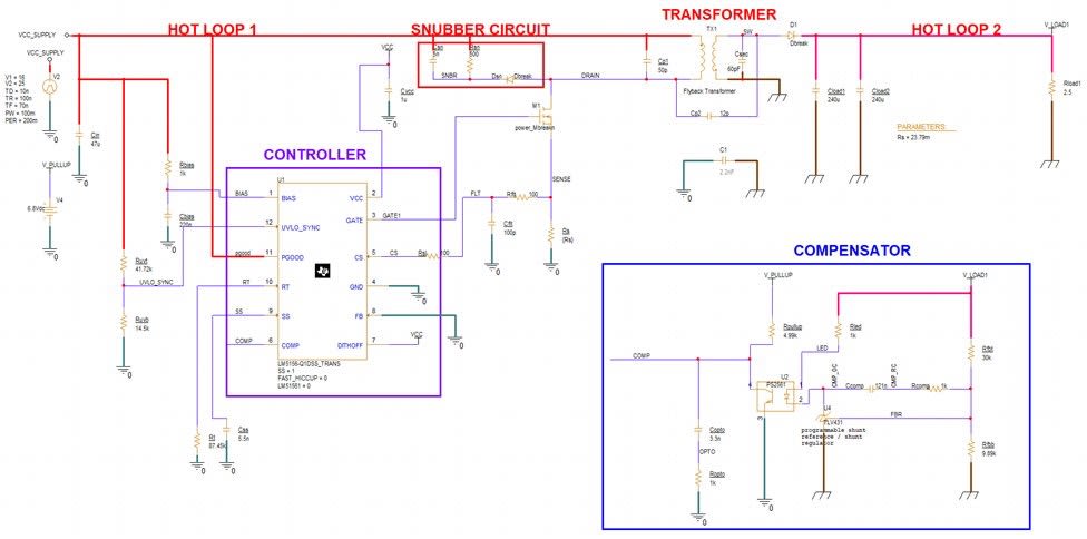
Figure 4. PSpice simulation schematic for a DC-DC non-isolated flyback converter using the LM5156-Q1. The snubber circuit handles the leakage inductance spike at switch turn-off. Hot Loop 1 and Hot Loop 2 are the high di/dt current paths that dominate radiated EMI. Minimizing their physical area is the primary PCB layout objective.
Operating Mode Is a Design Input, Not a Result
Select your operating mode before flyback transformer design begins. Core size, turns ratio, winding strategy, and compensation topology all follow from it. Changing operating mode after the transformer is wound means starting over.
Discontinuous conduction mode (DCM) fully discharges transformer energy each switching cycle. The control loop has a single dominant pole and compensation is straightforward. The cost is higher peak and RMS currents, typically two to three times higher than CCM at equivalent power, which increases conduction losses, raises output ripple, and demands more from the output capacitors.
Continuous conduction mode (CCM) reduces peak currents and suits higher power levels within the flyback range. The control challenge is a right-half-plane (RHP) zero in the loop transfer function. The RHP zero limits your achievable crossover frequency and requires a two-pole two-zero compensator. A compensator that is stable at one load point will not automatically be stable across the full load range. CCM designs that skip AC analysis at multiple operating points fail in the field.
Boundary conduction mode operates at the transition between DCM and CCM. Zero-current switching at turn-on eliminates reverse recovery loss. The penalty is variable switching frequency, which complicates EMI filter design. There is no fixed fundamental to attenuate and your filter has to work across the full frequency range. Select your mode before you select your core.
Return Current Does Not Go Where You Think
High-frequency return current does not take the path of lowest resistance. It takes the path of lowest inductance, which means it flows directly underneath the outgoing current trace on the ground plane.
A ground plane cutout, mounting hole, or plane split that interrupts this path forces return current to detour. The effective loop area increases. So does radiated EMI. This is not a marginal effect. The difference between a tight hot loop and a large one often determines whether a design passes or fails a radiated emissions scan.
The hot loop is your primary radiated emissions source. It is the high di/dt path formed by the primary switch, flyback transformer primary winding, and input capacitor. Minimizing its physical area is the layout objective that governs placement of those three components relative to each other in switch mode power supply design. Keep the transformer close to the bulk capacitor and the primary switch close to both. When signal traces change layers, place stitching vias adjacent to the via so return current has a direct path to follow. Everything else in the PCB layout follows from that.
Sigrity X return path analysis shows where current actually flows on your ground planes. Gaps and detours that are invisible in a visual inspection of the layout appear immediately in the current density map. Find them before fabrication.
Safety First. Then EMI.
Your isolated AC-DC flyback needs to pass two categories of certification before it ships.
Safety testing under IEC 62368-1 checks creepage and clearance distances, dielectric withstand across the isolation barrier (3000VAC for reinforced insulation), leakage current through isolation capacitance, and component temperatures under load. You cannot ship a product that fails safety. Creepage and clearance violations are the most preventable failure mode. A constraint-driven PCB design workflow that enforces spacing rules during layout eliminates this class of error entirely.
EMC testing under CISPR 32 and FCC Part 15 checks conducted emissions from 150kHz to 30MHz and radiated emissions from 30MHz to 1GHz. Conducted emissions is typically the harder test to pass. Input filter design, specifically common-mode choke selection and X/Y capacitor placement, determines your conducted emissions floor. An under-damped snubber that rings at a harmonic of your switching frequency will show up directly in the radiated emissions scan. Fix the snubber before you go to the EMC lab.
The sequence is isolation first, then conducted EMI, then radiated EMI.
Two Guides, One Topology
The flyback converter applied to an AC-DC isolated power supply and the flyback converter applied to a DC-DC problem share an operating principle and very little else in terms of design priority.
The Building a Quiet AC-DC Isolated Flyback in Allegro X covers the isolated design end to end. It walks through flyback transformer design with interwinding capacitance modeling for accurate PSpice simulation, constraint-driven creepage and clearance enforcement in Allegro X, RCD clamp design, Sigrity X return path and IR-drop analysis, and a practical compliance sequence for IEC 62368-1 and CISPR 32. This is the guide for designs that operate from AC mains and must pass safety certification.
The DC-DC Non-Isolated Flyback Design Using the LM5156-Q1 covers flyback transformer design, transient simulation, loop stability analysis, switch voltage stress and safe operating area evaluation, and PCB layout for DC-DC converter applications where power supply isolation is not required.
If your design operates from AC mains or requires a certified isolation barrier, start with the first guide. If you are working from a DC input source, start with the second.