PCB Layout Efficiency with OrCAD X Tools and Workflows
Key Takeaways
- Effective PCB layout efficiency hinges on customizable tools and workflows.
- Predefined menus, modifiable toolbars, real-time feedback, and advanced routing methods streamline the PCB design process.
- Proper component placement, dedicated power planes, and early design rule checks enhance overall layout efficiency and signal integrity.
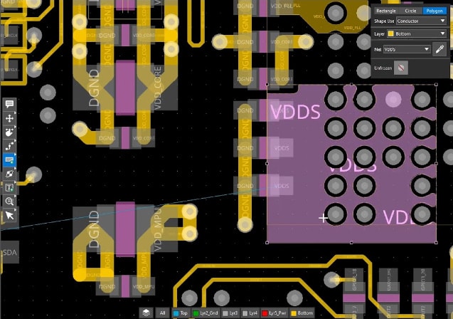
Adding and drawing shapes is made easy in OrCAD X.
Nowadays, design workflows may vary between projects. Different designers may have different needs, wants, and workflows needed to create their boards, depending on their individual preferences and the project they're working on. This is why, to achieve significant improvements in PCB layout efficiency, the name of the game is customization and reusing prevalidated design elements.
PCB layout efficiency encompasses the tools, features, and elements of PCB software that aid in creating an effective layout in as few steps as possible. This includes minimizing mouse clicks, with a customizable workflow that would fit a designer and features that allow for easy design reuse. Below, we discuss concrete elements of PCB design software, including design reuse, and how they aid in PCB layout efficiency.
Essential Features For PCB Layout Efficiency
|
Feature |
Description |
|
Design Reuse |
Reusing proven constraints and design modules accelerates the design process by reducing errors and ensuring consistency across designs. This leads to faster production cycles and maintains high quality by leveraging previously validated constraints and modules. |
|
Modern PCB designers require tools that can be customized for specific functions and workflows, rather than a one-size-fits-all approach. |
|
|
Specific Workflows |
CAD systems should allow the organization of commonly used commands into specific workflow menus, reducing the need to search through extensive menus and easing the design process. |
|
Customizable Toolbars |
Designers benefit from configuring toolbars to display only the necessary commands, reducing clutter and improving efficiency. |
|
Configurable Commands |
The ability to save command configurations, such as design rules checks, is essential to avoid repetitive setup for each use. |
|
Add-on Features and Utilities |
Incorporating custom commands and utilities, often created through scripting, can enhance productivity. However, having pre-made add-ons available can save time for designers. |
Workflow Changes for Layout Efficiency
Designers benefit from workflows that enable them to organize frequently used commands into a specialized menu tailored for specific tasks. Instead of navigating through a menu with numerous commands, designers can quickly access a simplified menu containing only their most commonly used commands.
Design Reuse for Layout Efficiency
Reusing designs in PCB layout workflows significantly minimizes errors and ensuring consistency across projects. By reusing validated design elements such as constraints, modules, and configurations, designers can avoid the frequent errors associated with manual entry. This practice saves time and enhances the speed and quality of the design process. Utilizing a PCB software that allows for design reuse thus leads to faster project completion and higher reliability in the final products.
Some commands, like design rule checks, require configuration each time they are executed. This setup can be time-consuming if done repeatedly. The ability to save command configurations allows designers to reuse the same settings, eliminating the need for repeated configuration and saving valuable time.
Managing Design Files
It is recommended to arrange your design files systematically. This approach will aid in team collaboration and ensure a seamless design for the manufacturing (DFM) process. Consolidating all design documents in a single location simplifies version control and minimizes the chances of errors during the design phase.
Visual graphic shown for customizable fanout and routing in OrCAD X.
Efficient Layout Design Tips
To enhance efficiency during the PCB layout stage, designers should prioritize proper component placement by grouping related components together and minimizing signal path lengths to reduce potential noise and improve signal integrity. Utilizing multi-layer stackups can help manage complex routing and provide better grounding.
To achieve efficient power distribution, it’s recommended to create dedicated power planes for different voltage levels within your PCB layout design. Implementing design rule checks (DRCs) early and often helps identify potential issues before they become costly to fix. Leveraging automated routing tools for less critical traces, while manually routing high-speed or sensitive signals, can balance speed and precision.
Visual graphics show the toolbar for easy place and route
OrCAD X For Layout Efficiency
The user-friendly environment in OrCAD X minimizes clicks to streamline PCB layout efficiency in addition to customization options:
- Design Workflows: Predefined menus for specific design technologies or tasks, which can be modified as needed.
- Design Reuse: The ability to import and export elements of prevalidated, known-good-designs such as constraint sets.
- Modifiable Toolbars: Customizable toolbars that can be configured to display only necessary commands.
- Configurable Commands: Commands whose settings can be saved and reused, enhancing efficiency.
- Productivity Toolbox: A set of additional features and utilities accessible for more complex tasks.
OrCAD X Features Specific to PCB Layout Efficiency
|
OrCAD X Features |
Details |
|
Design Reuse in the Constraint Manager |
The constraint manager significantly streamlines the design reuse process by facilitating the import and export of constraint files. This feature allows designers to easily apply proven constraints from previous projects to new designs, ensuring consistency and reducing the risk of errors. |
|
User-Friendly Environment |
Settings, commands, and design data are easily accessible, reducing the number of clicks and need to navigate through multiple menus. |
|
Grids and Snapping Configurations |
Quickly toggle grids on/off, define custom grids, or switch between common grids. Multiple snapping configurations for precise component placement and routing. |
|
Shape Management |
Add and edit shapes easily, similar to PowerPoint. Select shape type, layer, and net. Switch between 2D and 3D views for better visualization. |
|
Properties and Search Panel |
Display element information in the properties pane. Use hyperlinks to populate the search panel with design data. Navigate and resolve DRC errors efficiently. |
|
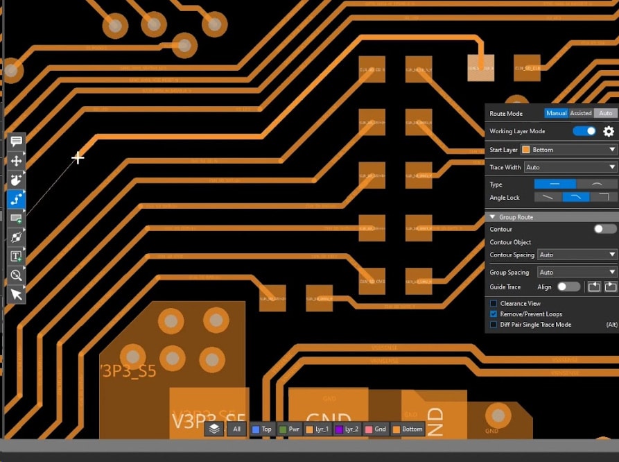
Routing Commands |
Access routing commands from a floating toolbar or use hotkeys. Switch between manual and assisted routing modes, adjust settings like hug, shove, and clearance. |
|
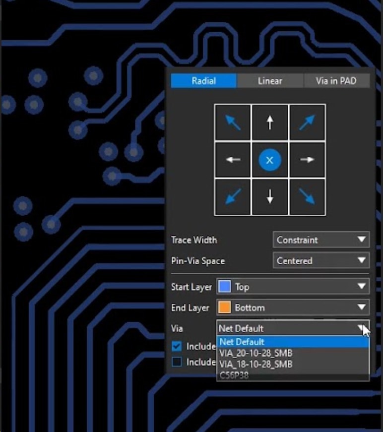
Fanouts |
Use visual graphics and previews for testing fanout strategies and via placement. Configure and add via arrays for signal integrity. |
|
Real-Time Feedback |
Allegro X powered routing engine provides real-time, constraint-driven feedback for manufacturable and functional PCBs. |
|
Clearance View |
Turn on clearance view to see spacing requirements and available routing channels, facilitating efficient routing. |
|
Routing Methods |
Use scribble, any angle, and neck mode for quick and easy routing through tight spaces. Contour routing for any flex circuitry to ensure bendability and minimal stress on etch. |
|
Design Rule Checks |
Immediate error generation with detailed information on electrical, physical, spacing, and manufacturing violations. |
|
Graphical Heads-Up Display |
Shows if length and timing constraints are being met, ensuring adherence to necessary constraints. |
|
Delay Tuner |
Adjust traces to meet requirements, improving routing efficiency for both simple and complex designs. |
To truly maximize PCB layout efficiency, customization of tools and workflows is essential. With OrCAD X, designers can tailor their environment to their specific needs. OrCAD X offers predefined menus, customizable toolbars, real-time feedback, and advanced routing methods, all designed to streamline the PCB design process.
Explore more about how Cadence tools can enhance your design process on our PCB Design and Analysis Software page and discover the powerful capabilities of OrCAD X.
Leading electronics providers rely on Cadence products to optimize power, space, and energy needs for a wide variety of market applications. To learn more about our innovative solutions, talk to our team of experts or subscribe to our YouTube channel.