PCB Design Layout Guidelines and Best Practices for Engineers
Key Takeaways
-
Follow standardized PCB design layout guidelines for consistent manufacturability.
-
Apply PCB design best practices early to optimize signal and power integrity.
-
Use CAD tools to manage library parts, stackups, and design rules efficiently.

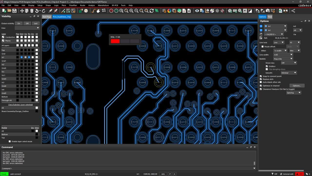
Trace routing should be done according to the PCB design layout guidelines for that board
A successful PCB layout balances performance and manufacturability by carefully managing libraries, CAD settings, placement, routing, and PDN design. Following best practices and layout guidelines ensures consistency, documentation, and system readiness.
Layout designers must ensure their work is fully documented and that the final product is ready for inclusion in the main electronics system for which it was designed. This is a lot of work though, especially for engineers who are new to the PCB layout process. To help with this workflow, it is a good practice to follow comprehensive PCB design layout guidelines and adhere to PCB design best practices from the start of the project. Industry and corporate standards will dictate the details of the design, but layout guidelines are important to help engineers navigate the board development process from start to finish.

PCB Design Best Practices Before Layout Starts
Before layout, several steps must be taken to ensure the design’s success; building the PCB footprint libraries is the first step.
|
Summary of Pre-Layout Steps |
|
|
Libraries |
Maintains the footprints for the board |
|
Board Outline/Stackup |
Defines the dimensions of the board in the x, y, and z-axes. The stackup also provides important electrical information such as the impedance profile |
|
CAD Parameters/Settings |
Users can customize certain visual and interactive features of the tool for an improved experience |
|
Schematic |
The controlling document for layout and part associations |
Libraries
When building libraries for PCB layout, it is important to use industry standards such as IPC or the manufacturer’s specifications for package sizes and dimensions. However, individual, corporate, or technology needs may also dictate changes in some of the parts. For example, footprints in RF designs may require smaller pad sizes than a standard digital design.
Some additional guidelines for building PCB component footprints:
-
Ensure that any library parts built have acceptable footprint sizes spaced according to the standard for that part.
-
PCB footprints need to contain all the necessary elements, such as part outlines, silkscreen markings, and reference designators.
-
A good rule of thumb is to ensure manufacturers can build the designed parts before committing them to the final design.
Another alternative is to use PCB footprints from external CAD library vendors. Part manufacturers often have their own components pre-built for a design system, and some tools have browsers to download these parts conveniently.
Board Outline and Layer Stackups
Having a good outline shape in place from the mechanical designer will greatly assist with the pre-layout planning stages. Although the form factor of the design can be changed later on, any alterations could force extensive redesigns of circuitry to fit the new shape. Also, most CAD tools will accept data imports from mechanical design systems, simplifying the process of adding the outline to designs. However, even with imported data, ensure that the board outline is correct and contains all of the necessary CAD elements, such as keepout zones.
Board layer stackups should also be finalized before the layout starts. Finalize and fine-tune the board stackup early to avoid costly redesigns and support impedance control. Choose materials based on key properties like dielectric constant and dissipation factor for accurate trace and signal integrity calculations. It is also important to select board materials at this stage so that proper trace width and other design calculations can be made according to the materials’ physical characteristics – dielectric constants, insulating qualities, moisture absorption rating, and dissipation factors.
PCB Material Comparison
|
Material |
Dielectric Constant (Dk) |
Insulating Quality |
Moisture Absorption |
Dissipation Factor |
Best For |
|
FR-4 |
~4.5 |
Moderate |
0.10%–0.20% |
0.020–0.025 |
General-purpose, low-cost boards |
|
Polyimide |
~3.5–4.2 |
High |
~0.15% |
0.015–0.020 |
High-temp and flexible designs |
|
Rogers RO4003C |
~3.38 |
High |
~0.06% |
~0.0027 |
RF and high-speed digital |
|
PTFE (Teflon) |
~2.1 |
Excellent |
<0.01% |
<0.001 |
Microwave & high-frequency apps |
|
Ceramic-filled PTFE |
~3.0–6.0 |
Excellent |
<0.02% |
0.001–0.005 |
Extreme RF, minimal loss |
CAD Parameters and Settings Best Practices
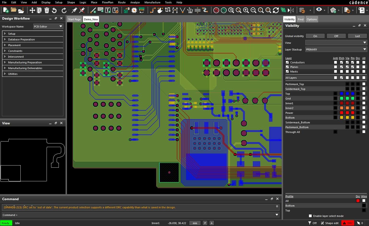
Many designers use default CAD settings, but customizing display options like colors, grids, and routing preferences can significantly improve efficiency with minimal setup effort.
PCB Design Best Practices for Schematic Setup
To make sure that all of the schematics have the same appearance, most companies will have internal drafting guidelines that typically include the following:
-
Schematic sheet size
-
Sheet border information such as company logos, name, address, date, part numbers, and revision numbers
-
Size and appearance of the grid to be used (establishes and maintains scale)
-
Symbol size and line widths
-
Text heights and font sizes
For the schematic development, these guidelines are often used:
-
Symbol spacing on the schematic sheet
-
Component information such as reference designators, part numbers, values, and pin numbers
-
Colors for net objects such as symbols, net lines, buses of nets, and text
-
Net spacing and naming conventions
Lastly, there will also be guidelines for checking and verifying the schematic through design reviews. Once the schematic has passed all of these processes, it is ready for PCB layout.

Setting up the display parameters of a CAD system is an important first step to PCB layout
PCB Design Best Practices for Placing PCB Components
With the CAD library, board outline, and other setup tasks completed, the design is ready for the layout to begin. The first step in this process is placing the PCB component footprints on the board. Three main requirements have to be met with the placement of components on the board: circuit performance, manufacturability, and accessibility.
Circuit Performance
High-speed circuits need to have their components as close as possible together for short and direct signal paths, but they aren’t the only components with this requirement. Analog circuitry and power components also need to be placed to make their sensitive or high-current lines as short as possible. This helps reduce inductance and increase signal and power integrity. However, these components may need to be spread apart to accommodate bus routing or thermal separation in some cases.
Manufacturability
To keep production costs as low as possible, it is important to place components in a way that they are as easily manufacturable as possible. For instance, components that are too close to each other may not be able to be automatically assembled or may have difficulty with automated soldering processes. Taller chip components preceding smaller parts into wave soldering can create a shadow effect, resulting in poor solder connections. Unbalanced copper between the two pads of small chip components can create uneven heating, resulting in one pad’s solder melting before the other one and pulling the other side up and off its pad.
Accessibility
Circuit boards often have to go through manual testing and rework, which requires access to the parts that need to be worked on. If other larger components overshadow these parts, it may make working on them more time-consuming or cause collateral damage to adjacent parts. Likewise, connectors, switches, and other human interfaces that aren’t accessible can also slow down the manufacturing of the circuit board.
One extremely important guideline is that placement should start with developing a basic floor plan of the parts on the board. Users may then strategize how to partition the different circuitry areas on the board to avoid overlapping analog and digital signals.

PCB Design Layout Guidelines for Routing
It is essential for circuit board designers to lay out boards to create the best signal and power integrity possible. Components should be arranged in the optimum position for short and direct trace routing. At the same time, the board must be laid out so that all of the nets can be completely routed. Trying to balance these needs can be quite a challenge in high-density designs. The first PCB design layout guideline is to set up the design rules and constraints for trace routing, which also aligns with PCB design best practices.
Design Rules and Constraints
Technically, configuring the design rules and constraints should have been included with the parameters and setup. But, since a large part of the rules applies directly to trace routing, this guideline has been included. Rules and constraints are used to govern trace widths and spacings and can be set up for individual nets, groups of nets called net classes, or as a default for all non-specified nets. Design rules are also used to control which vias are selected for different nets, trace lengths, and matched lengths, and which board layers are allowed for routing specific nets and routing topologies. Additionally, design rules are also used to control component spacing, silkscreen rules, mechanical clearances, and a host of other constraints.
|
PCB design rules and constraints must be set up before the circuit board layout to ensure the proper physical parameters are met for performance and manufacturability. |
Signal and Power Integrity
For maximum performance and signal integrity, PCB layout designers need to follow specific requirements for routing traces of different circuitry. Here is where the design rules and constraints will help by allowing designers to input the physical routing parameters into the CAD system for routing. Although the exact values will change depending on the needs of the board, designers will usually set up rules to ensure that the following guidelines are followed:
-
Short and direct high-speed transmission line routing
-
Trace width, spacing, and allowed board layers for controlled impedance routing
-
Specified trace lengths and length tolerances for matched length routing
-
Differential pair trace widths and spacing requirements
-
Width and spacing for sensitive signals such as clock and control lines
-
Via types for different nets
-
Trace widths and spacing for analog circuitry
-
Trace widths and copper weight for high-current power circuits
Another important guideline to remember is that when routing traces in mixed-signal designs, avoid crossing areas of digital circuitry with analog traces and vice versa.
At A Glance: PCB Routing Rules Best Practices
|
Signal Type |
Trace Width |
Spacing |
Notes |
|
High-speed digital |
Calculated for impedance (e.g - 50Ω) |
≥3W (3x trace width) |
Keep traces short and direct; maintain controlled impedance |
|
Analog signals |
Standard width (e.g - 6 - 10 mils) |
≥3W (or more for sensitive signals) |
Avoid routing near noisy digital areas; use ground planes |
|
Power traces |
Based on current and copper weight |
Follow IPC-2221 for voltage spacing |
Use wider traces for higher currents; consider power planes |
Guidelines for Effective Power and Ground Planes
With modern high-speed designs, the best grounding strategy is typically to use one or more continuous ground planes on an internal layer. This gives the best protection from EMI and ensures clear signal paths, which will improve overall signal integrity. Avoid routing traces across any ground voids for areas where the ground plane is broken up due to unique board contours or features. Noise can result from a lack of a continuous and adjacent ground plane to a signal plane and lead to circuitous return paths with large loop areas, resulting in significant EMI. Here are some effective power and ground plane guidelines:
-
Ground planes need to be adjacent to signal layers in the board layer stackup with high-speed routing. This will help shield the high-speed routing from interference and provide a good reference plane for the signal return paths.
-
Thermal relief pads need to be used and carefully managed for power and ground connections to the planes. The relief pad spokes must be wide enough to conduct high currents while eliminating those connections’ chances of acting as a heat sink.
-
Plan power connections and split power planes carefully to ensure the power is adequately delivered to all the connected parts throughout the circuit board.

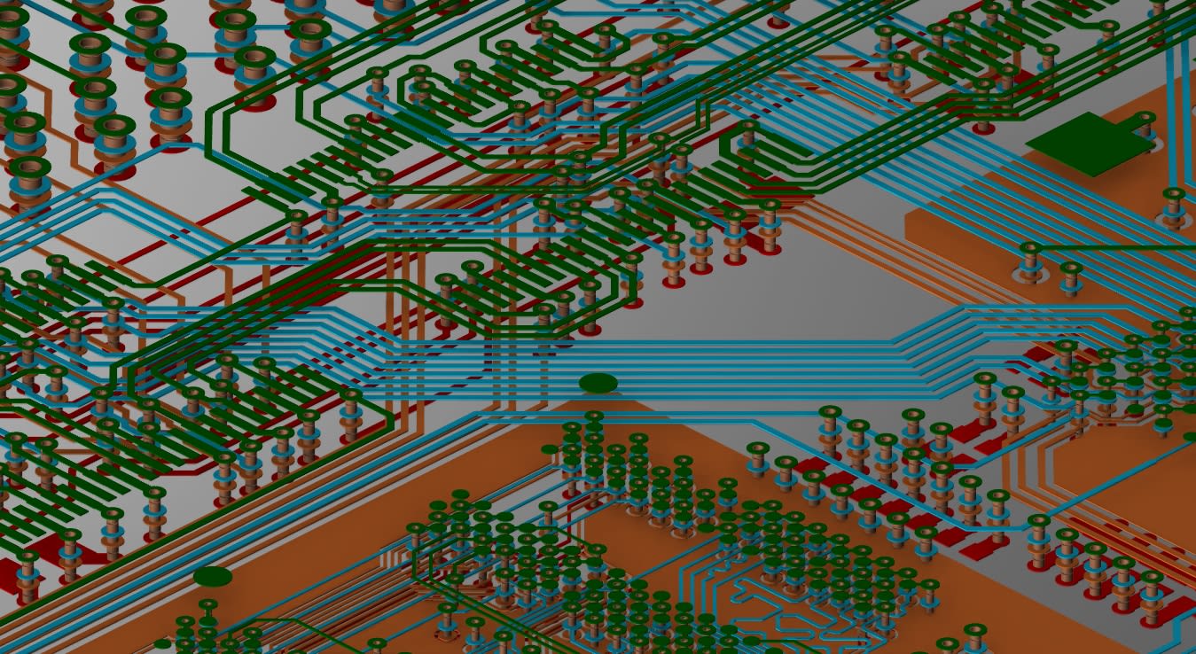
Avoid routing analog and digital circuitry together in a mixed-signal design
Silkscreen and PCB Test Guidelines
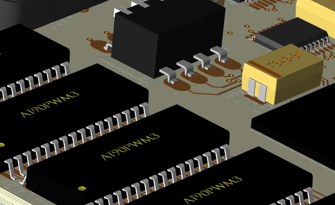
With the circuit board design completed, it is time to finalize the layout by cleaning up the silkscreen layers and adding testpoints. Reference designators, part numbers, and other corporate information are marked in ink on the circuit board through a silk screening process. Designers typically use “silkscreen” layers in CAD systems for designing these markings.
To ensure silkscreen layer markings are readable, designers follow these guidelines:
-
Line widths should be no smaller than 6 mils
-
Font sizes should be no smaller than 50 mils
-
Rename component reference designators according to a corporate grid pattern to help locate specific parts on the board
-
Move and rotate the reference designators so that they are easily readable
-
Include polarity and pin one marking where needed
Testpoints are essential for circuit boards that will be mass-produced for automated assembly validation. Each net in the design should have a testpoint on it, whether that testpoint is an existing thru-hole pin, a via, or an added surface mount testpoint pad. Testpoints should have at least a 50 mil clearance to other board objects, such as components or pads, and be at least 100 mils from the edge of the board. However, these values are likely to change from vendor to vendor, so be sure to check first what the manufacturer’s testpoint requirements are.
Guidelines for PCB Manufacturing Files
The last PCB design layout guideline is to create the manufacturing files for fabrication and assembly and send those files out to vendors. Output files are often automatically generated by scripts developed by designers or an internal CAD department. Most PCB design CAD tools, like Cadence’s Allegro X PCB Editor, have built-in creation tools available for use. Many tools also have functionality that communicates directly with PCB manufacturers through the IPC-2581 format. These unique features provide automatic transfer to a manufacturing database of fabrication and assembly files without the need to create and send each file individually.
By following proven PCB design layout guidelines and implementing PCB design best practices, engineers can optimize performance, manufacturability, and reliability from the start with Allegro X. To learn more about how Cadence tools can streamline your PCB design process, explore the Allegro X Design Platform by requesting a free trial.
Leading electronics providers rely on Cadence products to optimize power, space, and energy needs for a wide variety of market applications. To learn more about our innovative solutions, subscribe to our newsletter or our YouTube channel.