PCB Design For Military & Aerospace Applications
Key Takeaways
- Adhere to IPC and MIL standards for documentation, manufacturing, and testing to meet military and aerospace requirements.
- Choose high-temperature laminates and protective coatings to withstand extreme conditions and environmental factors.
- Design for higher current capacity with shorter traces and heavy copper (3-4 ounces per square foot); maintain a low aspect ratio (1:10 or less) for stability.
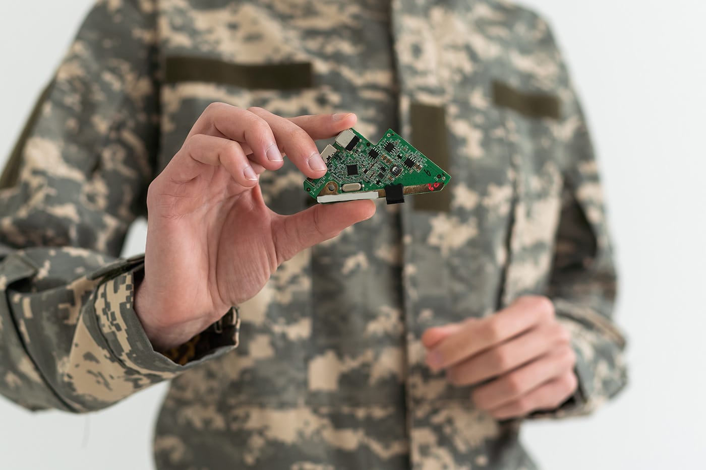
PCB design for military applications requires stringent standards and high-quality materials.
Military and aerospace PCBs must adhere to intensely high standards to ensure their safety and functionality in the extreme conditions they're used in. For this reason, PCB design for military and aerospace applications requires incredibly stringent guidelines with built in redundancy, extra safety, and stringent tolerances, minimizing risk of failure.
General PCB Design Tips for Military and Aerospace Applications
|
Category |
Tips and Considerations |
|
Component Selection |
|
|
Current Capacity |
|
|
Aspect Ratio |
|
|
Plane Separation |
|
|
Signal Protection |
|
|
Annular Ring |
|
Performance and Testing Standards for Military & Aerospace Applications
In PCB design for military & aerospace applications, adhering to standards is critical. Key IPC documents such as IPC-2610 Series, IPC-D-325, and IPC-J-STD-001, including the Space Addendum, provide comprehensive guidelines for PCB documentation, manufacturing, and assembly. Specific applications, including those for the Navy, FAA, and satellites, require compliance with IPC standards for materials and stack-ups.
Performance and testing standards such as MIL-PRF-50884, MIL-PRF-31032, MIL-PRF-55110, and MIL-PRF-19500 are mandatory for military PCBs, while AS9100 and AS9100D apply to aerospace PCBs. Additionally, compliance with the International Traffic in Arms Regulation (ITAR) is essential for military and aerospace PCB assembly. Regulated by the Department of State, ITAR mandates strict control over sensitive information related to the design and production of military and intelligence devices, ensuring the highest level of security and reflecting current technological, political, and security climates.
Wrap Plating
Wrap plating involves extending copper plating from the drilled hole onto the board surface. The IPC-6012 and IPC-A-600 standards define three classes for electrolytic hole plating thickness:
- Class I: Thickness agreed upon between user and supplier (AABUS).
- Class II: Continuous wrap plating through filled plated holes, extending onto the PCB surface, with a minimum thickness of 5 μm [197 μin]. Processes like planarization should not reduce this thickness.
- Class III: Minimum wrap plating thickness of 12 μm [472 μin] for through-holes and vias greater than 2 layers. Buried via cores require at least 7 μm [276 μin], and blind/buried microvias need a minimum of 6 μm [236 μin].
Challenges in wrap plating include knee cracking from thermal cycles, butt joint failures, and maintaining minimum thickness standards during the planarization process, which can vary by ±0.3 mils.
Military & Aerospace Applications Require PCB Design for Harsh Conditions
|
Category |
Tips and Considerations |
|
Acceleration and Vibration |
|
|
Lightning Protection |
|
|
Radiation Effects |
|
|
Packaging Challenges |
|
|
Test Coverage and Access |
|
Material Considerations for Military & Aerospace Applications
|
Category |
Tips and Considerations |
|
Resins and Foils |
|
|
Moisture, Salt, and Sand Effects |
|
|
Conformal Coatings, Potting Compounds, Staking Compounds |
|
Conformal Coating
For extreme operating conditions, choose PCB finishing materials like electrolytic nickel gold, ENIG, chemical silver, HASL, and lead-free HASL. Conformal coatings protect against heat, humidity, water, and vibrations, crucial for aerospace applications. Additionally, applying an acrylic-based spray protects the PCB from contamination and short circuits.
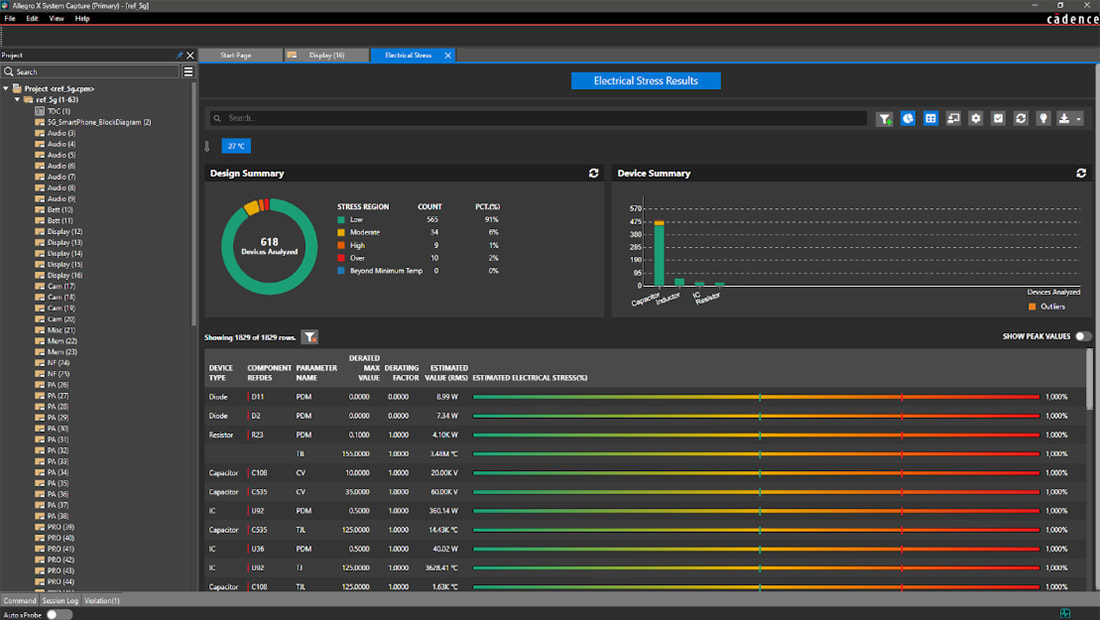
Allegro X System Capture is a comprehensive tool for PCB design, particularly suited for high-reliability applications such as military and aerospace. The tool integrates various analyses to ensure the robustness and reliability of PCB designs under extreme conditions.
Allegro X Aids in PCB Design for Military & Aerospace Applications
Allegro X provides Electrical Stress Analysis, which helps in identifying components that might be operating beyond their safe limits, ensuring that the design can handle worst-case scenarios. The key features include:
- Partitioning the PCB Circuit: The design is divided into multiple subcircuits, making the analysis more manageable and accurate.
- Parameter Calculation: It calculates parameters like power dissipation, voltage, and current for various components, including mixed-signal, analog, digital, and RF components.
- Derating Reports: The tool generates derating reports, which predict the circuit performance under worst-case conditions, helping in ensuring the longevity and reliability of the components.
Electrical Stress Analysis Results Dashboard within Allegro X System Capture displaying the design summary and estimated stress for all the devices analyzed.
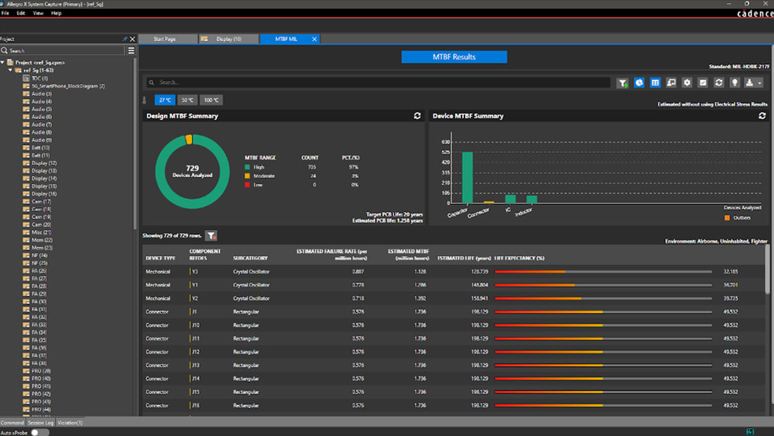
Allegro X Design for Reliability
For aerospace applications, reliability is paramount. Allegro X supports various analyses to ensure the reliability of the PCB design:
- Mean Time Between Failures (MTBF) Analysis: This estimates the durability and safety of electrical and electro-mechanical parts. The tool supports standards like MIL-HDBK 217F and FIDES for real-time reliability analysis.
- Power Topology Analysis: This validates the power distribution network across the PCB, ensuring that all components receive adequate power without causing excessive heat or voltage drops.
- Thermal Analysis with Celsius Thermal Solver: Integrated thermal analysis allows for early detection of potential thermal issues, helping in optimizing the placement of components and ensuring effective heat dissipation.
MTBF Analysis Results Dashboard within Allegro X System Capture displaying the design summary and estimated life expectancy of the PCB.
For more details on how Cadence tools can help in PCB design for military and aerospace applications, visit the PCB Design and Analysis Software page. Discover how Allegro X can enhance reliability, and ensure compliance with industry standards.
Leading electronics providers rely on Cadence products to optimize power, space, and energy needs for a wide variety of market applications. To learn more about our innovative solutions, talk to our team of experts or subscribe to our YouTube channel.