The Pros and Cons of Being a PCB Designer
So, you want to be a board designer? PCB Design is often referred to as "embedded engineering" Much like an Embedded Software Engineer who creates the code underpinning everything that is not considered a computer, the PCB Designer works in anonymity. Those line cards that connect telecom equipment to the backbone of the internet are an example where everyone uses the hardware without knowing anything about it - or the person who enabled it.
Nobody Knows Your Name - Except the People You'd Rather Not Hear From
Meanwhile, somewhere, in some factory, the drawings and artwork created around a PCB design will include your name at the top of the title block's Drawn By section. That's less about fame and more about blame. Among the manufacturing cohort, your name will be noted when a data point is ambiguous or left out altogether. They will contact you. The joke is that the contact usually happens on Friday night around 8:45pm. They're buying time?
You end up fixing other peoples' messes
Setting DFx aside, there isn't much recognition or respect for the designers. If you don't happen to have the EE chops to be the author of the schematic, you're just fleshing out someone else's work. They would do it themselves if they had the time. That is often the perception. Do this job for a while, and you will come to the conclusion that people overestimate their ability to do the layout in general and create a coherent document package in particular. You end up fixing other people's messes.
You Never Really Reach the Top of the Learning Curve
When I started in this business, it was by way of a trade school. Mary Sugden ran The Copper Connection. We had a six-month program where we started with analog basics and manual drafting. The conclusion of the coursework introduced CAD tools and digital design work. We were in the classrooms for 30 hours a week so around 750 hours total plus any homework assignments. 
Figure 1. Reading is fundamental. Learning new things keeps our minds sharp while preparing us for the next phase of our careers. Image Credit: Author
Earning a Bachelor of Science degree in Electrical Engineering would take almost three times that amount of coursework. It gets increasingly harder as you go so that path isn't for everyone. When I started out, CAD tools were not part of the BSEE curriculum.
Times change. The younger engineers would have gotten some training on the computer. In some cases, it would be just enough to be dangerous. Other colleges will do a deeper dive into ECAD layout. It could be anything from a chapter to a semester-long course on PCB Design.
There are a few ways to learn about PCB design online. Videos and tutorials are available. Some are free while others require a subscription. No matter what, you have to keep learning if you want to keep on working. There are PCB Designer certification programs. Going into those fresh off the street will be difficult. They generally distill the IPC documents into coherent chapters so a familiarity with the root documents is a plus.
Designing For Every Phase of Productization
Circling back to DFx, this is what separates the PCB Designer from the Electrical Engineer. Design For Manufacturing is the core discipline. We have to know what the fab shop can do. More importantly is what it can't do and that can and will vary from one vendor to another.
We speak to them by way of IPC standards. We listen to the vendor(s) by way of their technology roadmap. We also learn from every DFM report. You can send your crucial board design to three vendors and receive three different lists of questions about the artwork. Expect a variety of deviated requests from IPC standards to be included with the DFM technical questions. Plating thickness in the via barrel is a common sticking point.
Answering Technical Questions From the Vendor(s)
Of course, there will be some overlap from one vendor to another. We have choices in terms of answering those questions. We can allow the vendor to fix the problems themselves or ignore them to "use as is." Finally, we can ask them to stand by for new artwork moving to another revision where we address the issues ourselves. They are happy to wait - while pushing out the delivery date. 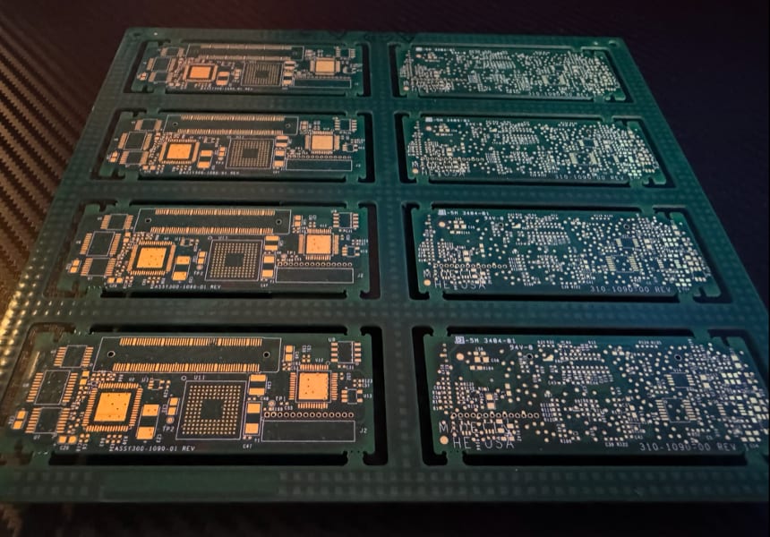
Figure 2. This 4-layer daughtercard gets stacked on a similar sized board. The stacking connector (right column, center-top) used considerable space on both boards. Initially, there were no components under the through-hole connector down in the corner. We added some parts at the last minute and I neglected to deal with the "MADE IN THE USA" on the silkscreen. The fab notes said to clip any text over the pads so that's what the vendor did. Even with that mistake, there were zero DFM questions; a bit of a rarity when going "100 miles per hour" to finish on time. Image Credit: Author.
Toggling over to Design For Assembly, the DFA requests can come in direct conflict to what the fabricator would prefer. It could be the PCB thickness tolerance, the allowable warpage or any other cost driver. Looking at the bottom line, I'd prefer a struggle in fabrication rather than taking a hit on assembly yields. It's about the money added in components as well as going further down the timeline. We have to find the sweet spot where each group is able to cope.
You could be working with a standalone PCB fabricator or one that is part of a vertically integrated Original Design Manufacturer or ODM for short. The ODM may even have PCB Design as a service housed within its capabilities. I used a captive service bureau like that for Google's virtual reality headset. We shared the effort on the main logic card and I handed off all of the flex circuits since those parts are well ingrained with the mechanical design effort. Don't be a hero, be humble and know your limits.
When Your End User is a Giant Corporation
When the design and production are all under the same roof, we call that an OEM or Original Equipment Manufacturer. The OEM will ultimately outsource the bare PCB through their Tier 1 supplier base. That business model, for instance, is characteristic of an automaker.
They would have Tier 1 suppliers who deliver completed modules whereas Tier 2 suppliers would be making sub components. for the Tier 1 outfits. The Tier 2 supplier would own the fab shop or have them as an exclusive partner. Finally Tier 3 suppliers would be the ones supplying raw materials to the fab shop and others.
When I was working on LiDAR sensors, that was a Tier 2 situation. Ford Motor Company was a key investor. They passed high level design requirements to us through their Tier 1 for that part. Included with that would be the requirements for component traceability and all sorts of other little details on how to properly run the business.

Figure 3. A point cloud that shows what a LiDAR sensor would "see" while doing Simultaneous Location and Mapping. This was generated with Velodyne's flagship VLS128 sensor. I redesigned all of the boards to increase functionality and assembly yield. The company founder and inventor of the technology had done the 1st iteration. I chose this view because I used to live right across the street. You can compare this to a streetview image of 382 South Redwood Ave., San Jose. Image Credit: Screen grab from a video: Velodyne Lidar Alpha Puck-Santana Row.
I had to spend a lot of time getting up to speed on Ford's documentation and process controls as part of their vendor management. We were compelled to pass that information down to our suppliers and make sure that they documented their compliance. Military programs go the same way.
The Spirit of Continuous Improvement
Big business requires more documentation that you have to learn and follow. This may include the Japanese philosophy of Kaizen and Kanban - continuous improvement through small steps in the right direction. Kaizen provides the overarching themes while Kanban works through the tangible details of never-ending improvement.
Some folks will be drawn to that level of regimentation, while others prefer to adlib their way through. That is where start-up companies come in. Hardly anything is written down. You learn the "tribal knowledge" one bit at a time. Sometimes, you are making up the rules to suit the needs of the company. Your downtime can be filled with generating procedures for different aspects of the design. That suits me just fine since I'm a good writer - or so I've been told.
You Can Do This Job From Almost Anywhere
The COVID-19 lockdowns were a blessing in disguise. The industry learned that we can be effective while working from home. As an older, established empty nester, I was in an ideal situation to dedicate a spare bedroom to an office. Unfortunately, some of you youngsters may not catch the same breaks. Having a stay-at-home parent is a luxury that I was proud to provide for the kids.
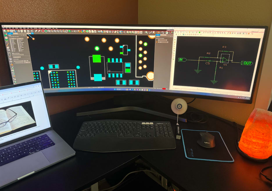
Figure 4. There is something to be said for having the largest monitor possible. While this is my home setup, smart companies will provide more desk space and a more powerful computer than the average employee will get. I've been in CAD caves that are perpetually dark and even one where we had remote controls to dim the overhead lights, exclusive to the CAD group. Image Credit: Author
On day-one of my time at Microsoft, my manager said that she was fine with me working from home. No thanks. I like free coffee and lunch and especially like someone to be there when I have a burning question. There was one such person throughout the week while a few more came in for the weekly staff meeting.
Perks Are What You Make of Them.
Note that free lunch is not normal there. I asked, "Are we coddled here in the Bay Area?" Yep. Alphabet is right there at the same exit, and they were spoiling us in every way possible. It wasn't even about lunch being free, just different. My wife and I are celebrating our 29th anniversary on August 11th, and I've eaten everything she knows how to cook, many times over.
That said, working at home is very nice. I've got a heat pad over my shoulders with a flap that goes up the back of my neck. Sweat bands shield my wrists from the edge of the laptop and mousepad. I can lie down for a bit or hop on my bike with no problem. I have my own shower. I've learned to appreciate all of that, along with the silence that goes with a closed door.
Writing all that to write this: carpal tunnel syndrome is real. A trackball may be kinder than a mouse. Either way, my survival strategy was to switch hands throughout the day while leaving the mouse configured for a right-hander. Left-hand dexterity was already there from playing guitar. Your mileage may vary; just be aware of the penalty for repetitive motion.
Shop around, you're in the driver's seat of your career.
Employment in the Bay Area has always been easy to find. This holds especially true if you can handle being a contractor. The benefits are not as good as a direct position but you increase your value at the end of every assignment. Some employers still embrace the work-from-home plan. My last job before retirement was hybrid work; the best of both worlds. Shop around, you're in the driver's seat of your career.
In Conclusion:
Printed circuit board design has been very good to me. I got in while Plated Through Hole technology was the only game in town. I got to learn about surface mount, high definition interconnect, exotic materials, substrate design and all kinds of cool things along the way. People going into the industry today will be expected to know that stuff going in. The employers will want that 4-year degree in electronics. From there, pile on the particular technology of interest to the employer.
Say what you will about that but it puts you on an even playing field with those who came up through on-the-job experience. I learned the language without having to do all of that math. Your education will open the doors to other types of work, including chip design, taking you places I could never go. I'm humbled to be able to write this since so many of you are educated beyond my capacity. Making a career out of PCB Design is a noble choice. The rest is up to you.