Are You a Little Board?
The whole world gets a little smaller and a little faster every other day. The underlying magic that supports this flow of knowledge is constantly evolving to keep up. The 5G rollout is still young and already, 6G the “Next Marketing Breakthrough” ™ is digging into the slideware trenches.
Our hardware has to answer the call to be anywhere and at any time. Our gizmos are an extension of ourselves. Every new Genie that springs from the bottle will lead to another wave of engineers crashing out their code. Those software heroes need the means to move all that lovely data. I looked at i-watches and was astonished to find the number of price points and other players in the game. Development boards feed the process on a continuous basis.
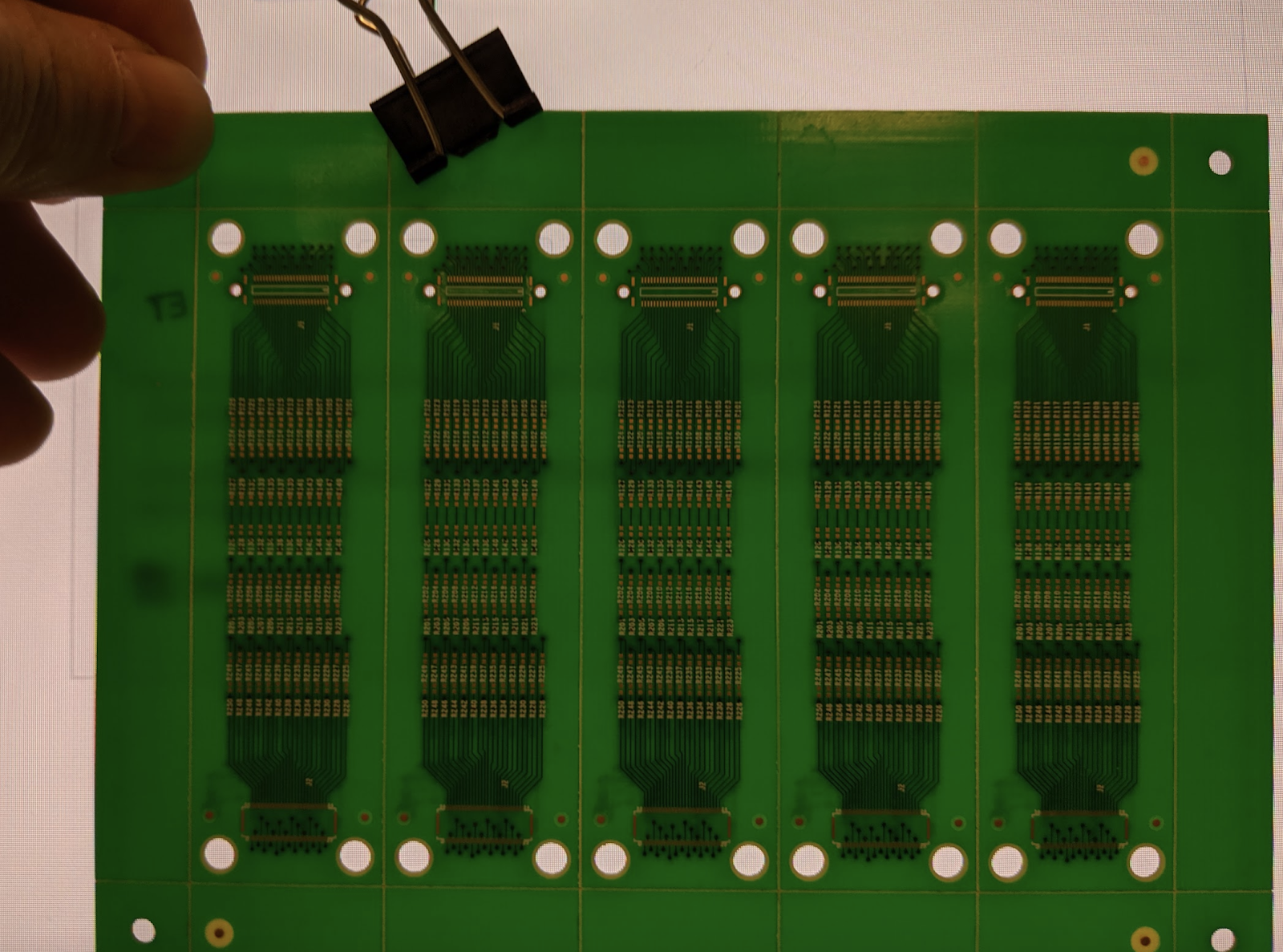
Image Credit: Author- An “oops” board to fix a pin-out mismatch.
That leads us to the little things in life. What wacky invention becomes the next must-have of the burgeoning consumer season in front of us? Not so much inventing new stuff, there is that and more, reinventing existing stuff so that it is worth more to the customer. Like clockwork, the new idea gets competition and the cycle repeats with cleaner packaging by the market leader to cement the brand. That’s when the chip-set members become a little more cozy with one another.
A little board and a lot of stuff will require us to find the right balance between cost and features. There is value in a one-sided board with through-hole vias. It’s relatively quick to fabricate and assemble. It would be thinner overall and easier to rework. The number of qualified vendors is in your favor with a single-sided board.
Honey! I Shrank The World.
When the walls close in, both sides of the PCB need to be populated. You may have to solder one side of the board with a high melting point solder and then use a lower temperature formula for the primary side. Another means is to glue down the heavier components on the secondary side and then run the boards through the oven once. Board with a mixture of surface mount (SMD) and through-hole (PTH) components are a candidate for one-shot soldering using pin in paste technology. Approach with caution.
Little comes in all sizes. A board gets small when there is more circuitry than normal. At some point, some things get left off. For instance:
-
Can the board fiducials relocate to the break-off areas of a subpanel?
-
Limit test access - 10% or fewer rather than 90% or more as the goal.
-
Silkscreen takes some creativity and could be cut short.
-
A designated spot for a solder blob instead of a no-stuff zero-ohm resistor option.
-
Of course, smaller parts. If the board can be placed, it can be routed.
Getting Embedded
Given the real estate shortage, someone had to decide to put parts inside the PCB. It is not as wacky as it sounds with the smallest components. To do these correctly requires a thick enough board and parts small enough to embed therein. Some of the technology borrows from the substrate business where die cavities are quite common.
A seal ring around the components on the layer where they are attached eats into the adjacent routing channels. No way in or out of the embedded zone except by micro-via from below. You wouldn’t place a component on an inner layer and then route away from it on that same layer. That’s one thing. There are a number of rules for whatever technology is used. Consult a well-known vendor; this is not a home brew solution.
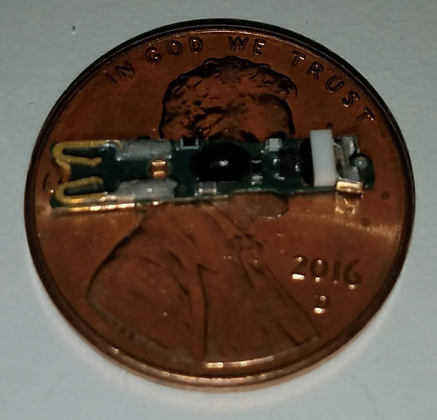
Image credit: Author - A four-layer board that can hide under a dime.
Another tangent is embedding capacitance as a structure between two metal layers and a dielectric between them. The structure of a printed circuit board works like a capacitor. The symbol for a capacitor, as you may know, graphically represents two metal plates and with a gap between them. Special dielectric materials allow for more embedded capacitance than FR4 materials. They can print resistors too. Squares of the material of different sizes provide small values of resistance. Embedded capacitance and printed resistors are not exactly mainstream but more so than embedding actual chip caps and resistors.
Going Modular
Modules are a natural resource for those inclined to the fast and small. Radios, power supplies, and memory modules are some of the usual suspects. The beauty of it is that you can have 0201 class components or high-speed material in that confined location. If you can’t find something off the shelf or you think you can do better, go for it. Designing an interposer, a daughtercard or a module is just another form of PCB layout.
Qualcomm has an income stream from custom RF modules that kept me busy with one little project after the other. It was like a homecoming when Google added me to the Pixel hardware team. Several years with QCOM never saw a Snapdragon device that had not already been fanned out. They would give me a break-out board for a revision and make sure that I knew not to touch the ‘dragon.
My fifth year at Google started off with removing the Snapdragon 835 SOC and replacing it with an 845 on the break-out board for the Pixel 3. Hint: they are not pin-compatible devices. It was a do-over. We were given a nice full-page power tree and a pin list with the current draw for each.
There were weeks spent tying the PMIC to the dragon before the design passed the simulation. A PMIC is nothing but a bunch of power supplies in one package. Picture a hoard of big inductors that need to go “right next to” the pin. I’m guessing that twenty separate voltage domains with any number of pins on each one. In addition to the typical phone hardware, we also wanted to monitor all of those domains to verify the simulations down the road. Most of the features were in modules though we did a discrete layout of NFC and few others.
A break-out board is a huge affair with the various pieces of the phone puzzle set up for debugging hardware, firmware, and code. I learned so much from that effort that it deserves its own story - one focused on big jobs; stay tuned! The point is that the future phone PCB’s are quite large at this point but already on the drawing board. They will have to take Occam’s razor to these monsters. Smashing the big one down to fit around the battery of a smartphone is a whole different thing. What else do you want your watch to be? With no unused space, It’s a small world after all.