Teaming Up For Success on a Large PCB Project
Time to market is often one of the most important factors in the success of a project. Capitalizing on a new idea while others are pursuing the same goal is much easier when your product is there first. On the contrary, the second-place finisher has to come in with more or better functions and at a lower price in order to take market share from the incumbent. That, in a nutshell, is why printed circuit board design is a critical job for any enterprise. Getting in while the margins are high provides the best return on investment. That’s what we want.
Face it, a good layout takes time. There is the logic capture, the physical outline, the electrical interface, power requirements, signal integrity and a host of other details that have to be integrated into this one vessel. Taking all of that information and producing a working product that people will buy is our goal. Failure to get the design win can sink a program or even bring an early end to a start-up. The pressure is on the Designer to meet the commitment to the market window of success.

Image Credit: Author: Everything starts with a dev-board
For that reason, we often start a job even though it is not fully defined in terms of the attributes listed above. When I know I’m working with an incomplete set of data, as is usually the case at the start, everything is a “study”. A placement study and then a fan-out study, a power distribution study, high-speed routing study and so on. The idea is to find the pain points of the design and work to clean those areas up.
Teamwork results in nearly double the output. Getting help with the studies puts another pair of eyes on the hot spots. That’s a key takeaway. The more organized places have a policy that enforces a buddy system where someone besides yourself has to sign off on the new or different component footprints used in your design. They’ll be back to look over the completed deliverables as well.
One of our prototype versions was great for silent movies.
It’s not foolproof but a lot of unforced errors have been brought to light during the “sanity check.” If you’re familiar with a ball-map of a BGA footprint, this will make sense. Every Chromebook needs an MLB, a main logic card to qualify. One of our prototype versions was great for silent movies. The datasheet for the audio decoder showed the ball map as though you were looking at it from the bottom. This is the opposite of the way we see things in our CAD system. You know where this is going. It was maybe an 80 pin device and the PCB footprint was completely “borked.” It was a happy ending for the audio engineer since we had one more proto-spin before launch.
As the data comes into focus, the clock has been ticking and the due date is fast approaching. New and improved generally translates to more circuitry and less room for error. The typical update has the physical design getting tightened up or the electrical side adding more stuff. As designers, we’re only good for about half of a day’s work; 12 hours. Then, we sleep it off and do it again.
That’s not enough anymore. Since we can’t work around the clock, we turn the job over to someone who can process the design overnight. That could be a teammate who heroically goes on swing or graveyard shift for the duration. Just as likely, an outside firm is brought on board to fill in while we’re away.
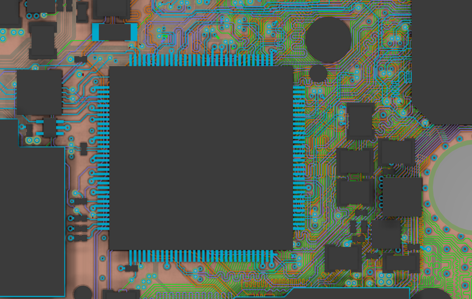
Image Credit: Author - Layer by layer or part by part, divide and conquer
Another approach is one we used at Qualcomm. We had a small team of Electrical Engineers in Taiwan who would work on the RF layout through their day and pass the wreckage on to me to turn their sketchy work into a legit layout. Mostly, that meant spreading things out to the minimum spacing after they mashed it all together.
Morning and night time hand-offs kept the job moving forward or at least appearing to move forward on their end. No, really getting their design intent and cleaning it up worked quite well for the most part. The development plan for a version of the recently sunsetted Daydream VR headset went like that except that there were real designers on the other side of the world who were sharing the design load.
Coexistence is a hard problem.
So that brings me to the Pixel development board. Google used the same Qualcomm flagship device for their top tier smartphones for 2019 as the Daydream unit. They came out in ‘19, right? In order to pull in the schedule, we resorted to splitting the board up into functional blocks. The divide and conquer method was used in addition to the time-shift plan as above. The first partition to spin-off was the wireless section. Not surprisingly, it was also the last to come back in. Coexistence is a hard problem.
Getting power in and signals out of the SOC was my part. A third designer would get their own evolving partition every day. This designer was part of a service bureau as was the overnight designer who had the whole board except the RF partition. There was some danger there where instructions may not have made the trip around the world every single night. As the overall owner, I had to spend more time coordinating the job with two stand-up meetings every day.
The first one was the full-stop where we could introduce new logic. Our schematic was hierarchical with the radios nested as an independent block. The other partition had to be reabsorbed so we could keep an eye on progress and make any adjustments to the boundaries. I basically never mention my sponsor here but Cadence gets some credit for enabling us to work as a team on this board.
There’s a learning curve for working with the partitions. All of the good features require effort to master so this is no exception. In addition to that, creating slide shows and otherwise collaborating with the remote team was a little distracting. I wasn’t getting as much done on the core of the board but more was getting done overall. In the end, it was a net benefit. The thing you can’t do is throw something over the wall and hope for the best. We work best when we work together. There’s your best hope.