PCB Design For Solder Mask Defined Footprints
Continuing with the shrinkage theme, it’s worth looking at a critical layer. Whether it a simple board or a major project, the solder mask can make or break the assembly line. As solder defects pile up, the rework required eats away at potential profit. With fierce competition for sales, the gross margins are usually thin as a matter of course. Even if you own the market of captive customers, getting more bang for the development buck is a win.
So, it comes down to the little things. PCB footprints with solder joints about the size of a colon (not the internal organ, the punctuation mark) leave little room for error. The discrete components that go on such small pads are themselves quite small. That makes the parts very light as well.
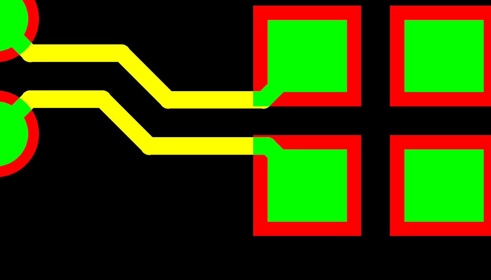
Image Credit: As line widths collapse, it’s easy to overlook the shorting potential where the green shape defines the actual pad. Flip the script and square it up.
When we put these featherweight components on the board it is normally done with a robotic hand squishing the part down into a dab of solder paste. The populated board goes into an infrared oven to reflow the paste and form a solder joint or, more precisely, two solder joints at the same time. The period when the solder paste is in a liquid state is held to a minimum so we don’t damage the board or the devices by extended exposure to the high temperature.
Library
The parts themselves come in all different sizes. The assembly traveler will note the minimum size or pin pitch as one of the primary factors. Bigger is better for the yield while smaller is higher performance. Finding the right balance comes down to the component form factors available to fill out the bill of material. You can usually find a quad flat pack solution for everything. Modern packages are finer pitch; what a surprise!
Sometimes the only game in town is a BGA package. They come in many flavors. The distinction beyond the sheer number of pins is the pin density. When the pins get crowded the normal PCB with plated through holes will no longer suffice. Enter HDI, high density interconnect featuring the “expensive” micro-vias you’ve probably heard about.
OG chip vendors went to great lengths to stay on the cheaper PCB technology. Seeing the upstarts make use of the shrinkage and facing the trend, perimeter leads or well-spaced arrays only get us so far. The writing was and is on the wall. Sub-micron chip technology is trending towards sub-nano-meter technology. It’s these boards and the ones with fine-pitch packages that are in play when we’re looking at solder mask defined lands.
The last viable node for BGA packages with through-hole technology is 0.65 mm pitch. Unless there are some relief rows of unpopulated pins to allow regular vias then 0.50 mm pitch and below will require the use of HDI boards. The next node down is a grey area. When we’re down to 0.4 mm pitch devices, we could still make a case for laying down 100 microns (0.1 mm) of solder mask between pads. This amount is the minimum you can expect to have and pass the adhesion test. Less than that is considered a sliver and is a no-no.
Back to the math. The 100 microns of mask taken from the 400-micron pitch leaves 300. Solder mask expansion, by the IPC statute, is also 100 microns but the secret is that the fab shops are mostly ahead of the spec on mask registration. We can get away with a 75-micron solder mask expansion leaving us with a finished pad diameter of 225 microns which is just enough to fit a micro-via in pad non-soldermask defined solution.
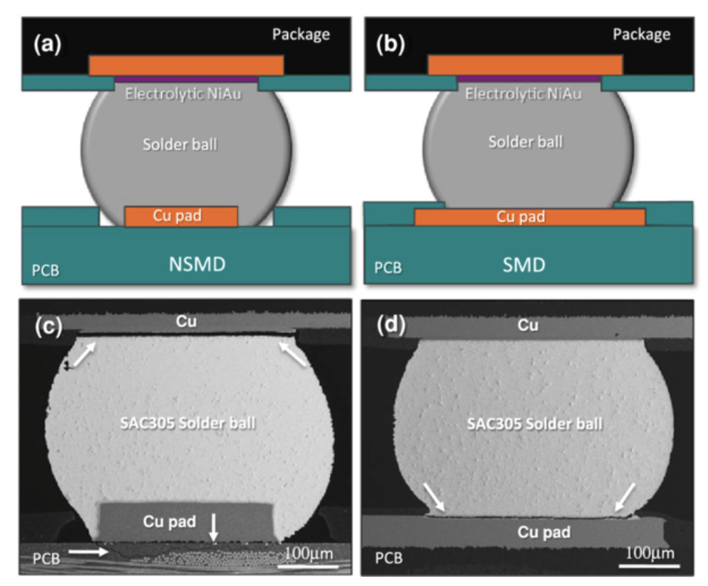
Image and quote credit: Research Gate
(a) non-solder mask defined (NSMD) and (b) solder mask defined (SMD) board-side pad design. An example of a NSMD laminate crack and a package-side crack (c, the laminate area contrast is modified to visually reveal the laminate crack), and a PCB-side Cu pad interface crack with the SMD pad design (d).
This NSMD geometry is preferred by most chip vendors as stated on the typical datasheet. If they show any preference at all it is likely to be for it rather than mask defined. It’s when the device maker says to consult your PCB assembly and fabrication representatives that you know that you’re on your own to come up with a viable solution. It will end up being a matter of teamwork and as much of it as it takes to implement the fine pitch components.
What if your stack-up requirements were such that a larger via is required? What happens when the 0.4 mm part is replaced by one that is 0.35 mm from pin to pin? Enter mask defined lands. The idea is to live with the 100-micron solder dam, lean into the remaining 300 microns with the metal layer and define the solder mask as a circle within that circle. The overlap works out to the same as the expansion.
Solder paste
All along, the aperture for the solder paste stencil matched the metal layer of the component footprint, the “pin”. It still can. Only the pin is defined by the solder mask layer. Flip the script in the padstack to go along. That said, don’t be too surprised when solder volume becomes a topic of discussion once the boards start going through the reflow oven. Squares of paste that overhang the mask or other techniques that increase the paste volume may be proposed by the assembly house.
Don’t take it hard if the best-laid plans go awry. Fine-tuning of the soldering process is a normal part of the growing pains as we start to scale. Adding mask defined pads to the tool kit is all but inevitable with the chip vendors racing to the bottom on size. Just as rigid boards are different from flexes, fine-pitch is another branch of knowledge to acquire. Thanks for following along.