Getting Started with PCB Design
Key Takeaways
-
Understand PCB layers, components, and types to guide your design decisions.
-
Follow the structured steps, from schematic capture to layout and review, for optimal results.
-
OrCAD X offers robust tools for both beginners and professionals.

Below, we outline the essential information needed to get started with PCB design.
Printed circuit boards (PCBs) are the foundation of modern electronics, connecting components to create functional devices. They consist of a flat board with copper traces that replace traditional wiring. These traces electrically connect components, enabling compact and reliable electronic designs. PCBs can range from simple single-layer boards to complex multi-layer designs for advanced applications. Read on as we explain all you need to know for getting started with PCB design.
Getting Started with PCB Design Basics
Before starting, it’s important to understand key concepts and types of PCBs to guide your design decisions.
Key Concepts and Terminology
-
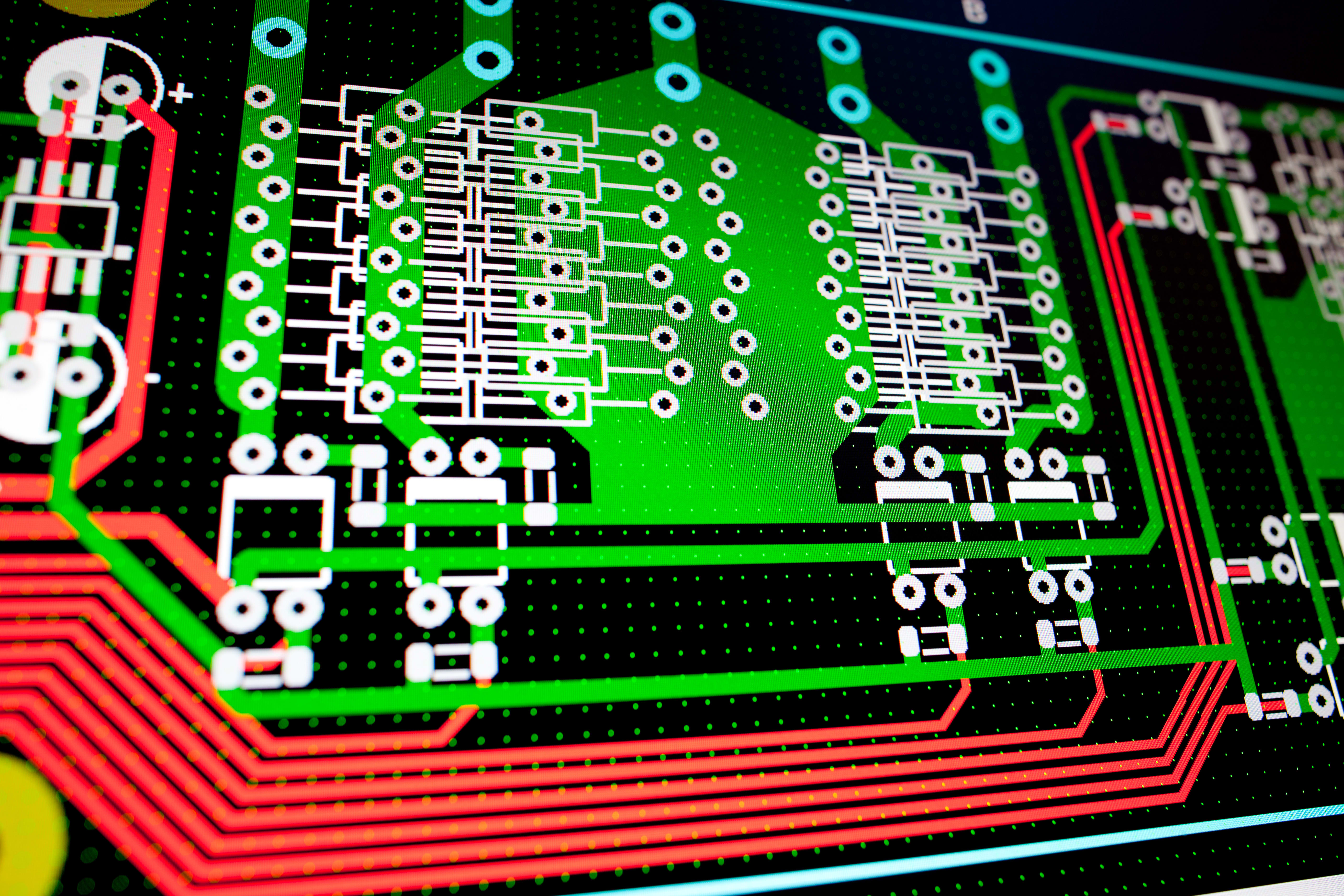
Layers: PCBs consist of copper layers for signal routing, a solder mask for protection (that covers otherwise exposed traces), and silkscreen for labeling. Multi-layer boards include additional layers for power or ground to enhance performance.
-
Traces, Pads, and Vias: Traces are conductive pathways, pads connect components to the PCB, and vias link signals between layers. Each plays a crucial role in routing and connectivity.
For more information about types of routing see our in-depth explanation here.
PCBs can be single-sided, double-sided, or multi-layer, best suited for complex designs. Rigid boards are most common, whereas flex boards are bendable for compact designs, and rigid-flex combines both for versatile applications.
Getting Started with PCB Design Software
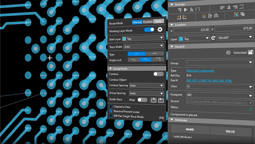
In getting started with PCB design, the first step is choosing a PCB design software, also known as ECAD software. This software allows you to create schematics, lay out the PCB, and export manufacturing files. Free tools are available online, as well as paid tools that are typically more suited for professional use.
OrCAD X is an exceptional "best of both worlds" software. It offers powerful capabilities, setting you up to work with industry-standard tools, while also being accessible to students with a free six-month trial. Widely used in professional environments, OrCAD X integrates seamlessly with other tools in the Cadence ecosystem, making it ideal for handling quick-turncomplex designs as well as for students and beginner engineers working on their first projects.

Key Steps in the PCB Design Process
|
Step |
Key Points |
|
1. Ideation & Requirements Gathering |
- Define project scope and objectives. |
|
2. Schematic Capture |
- Create a circuit diagram using CAD software. |
|
3. Component Selection & Library Management |
- Choose components based on availability, cost, and performance. |
|
4. Board Layout |
- Import your schematic into a PCB design tool. Many ECAD softwares can handle both |
|
5. Design Rules & Constraints |
- Set trace widths, clearances, and via sizes according to specifications. |
|
6. Grounding & Power Distribution |
- Implement stable power and ground planes. |
|
7. Signal Integrity Considerations |
- Manage impedance and length matching for high-speed signals. |
|
8. Review & Verification |
- Perform Electrical Rule Check (ERC) and Design Rule Check (DRC) in CAD software. |
Getting Started with PCB Design Prototyping and Manufacturing
After finalizing the design, prepare files for manufacturing and choose a suitable fabrication partner. Your ECAD software should be able to handle any necessary exports for your desired file types.
Choosing a Manufacturer
-
Local vs. International Options: Local manufacturers offer faster turnaround times but may be costlier, while international options, especially in Asia, are often more affordable.
-
Cost and Lead Times: Prototype services offer quick production for a higher cost, while large-scale orders reduce unit prices but require longer lead times.
Assembly & Soldering Basics
-
Surface-Mount vs. Through-Hole Components: Surface-mount components are compact and common in modern designs, while through-hole components are used for larger parts or prototyping.
-
Hand Soldering and Reflow: For prototypes, hand-soldering is common, but reflow ovens are better for small production runs. Proper technique ensures a reliable connection.
Prototyping is your chance to test and validate the design. Identifying and addressing issues at this stage ensures your final product is robust and functional.
If you're getting started with PCB design, OrCAD X provides a comprehensive suite of tools to streamline the process, from schematic capture to layout and manufacturing. Whether you're a beginner or a professional, OrCAD X ensures reliable designs with an industry-standard software. Explore how OrCAD X can simplify your PCB design journey by visiting PCB Design and Analysis Software and the OrCAD X platform.
Leading electronics providers rely on Cadence products to optimize power, space, and energy needs for a wide variety of market applications. To learn more about our innovative solutions, talk to our team of experts or subscribe to our YouTube channel.