Differential Pair Length Matching Guidelines
Key Takeaways
-
Length matching reduces timing skew in high-speed differential signals. Material properties like dielectric constant and fiber weave impact propagation delay and skew in differential pairs
-
Use meandering, accordion patterns, and symmetrical vias for accurate length matching.
-
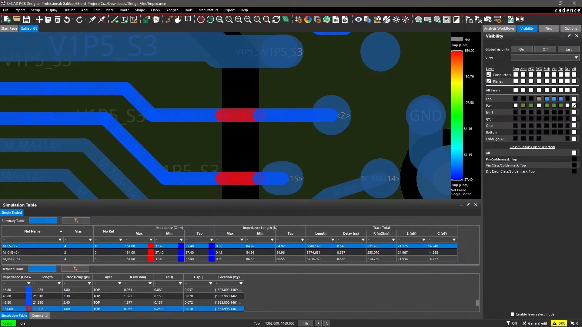
OrCAD X supports differential pair constraints, real-time phase monitoring, and impedance tuning for precise routing.

Differential pair routing on a printed circuit board
Differential pairs are mostly used in high-speed digital and analog communication technologies. Some examples include:
-
High-speed data interfaces: USB 3.x, USB4, HDMI, DisplayPort, SATA, PCI Express (PCIe), Ethernet.
-
Memory interfaces: DDR4, DDR5, and beyond.
-
Serial communication standards: LVDS, RS-485, CAN, SerDes interfaces.
-
RF and microwave circuits: High-frequency signaling and RF front-ends.
The fundamental reason for length-matching differential pairs is to ensure both traces experience similar propagation delays, minimizing timing skew. Timing skews the difference in signal arrival times at the receiver. Excessive skew reduces the effective noise cancellation properties of differential signaling and increases susceptibility to interference, ultimately resulting in reduced signal integrity. Below, we’ll discuss differential pair length matching guidelines to ensure your board is ready for high-speed, and how OrCAD X aids in accomplishing this.
Design Parameters for Differential Pair Length Matching
Differential pair length matching guidelines include skew limits, and typical recommended skew limits depend on signal speed and protocol. Common guidelines include:
|
Signal Speed Category |
Frequency Range |
Allowed Skew (mils) |
Allowed Skew (mm) |
|
Low-speed |
< 100 MHz |
±100 mils |
±2.54 mm |
|
Moderate-speed |
~100 MHz – 1 GHz |
±25–50 mils |
±0.635–1.27 mm |
|
High-speed |
> 1 GHz |
±5–10 mils |
±0.127–0.254 mm |
|
Ultra-high-speed (multi-GHz) |
Multi-GHz |
±2–5 mils |
±0.05–0.127 mm |
Impedance Matching for Differential Pairs
Differential impedance matching (typically 90–100 Ω differential impedance) is just as important as length matching. Design factors affecting impedance include
-
Trace width and thickness.
-
Dielectric constant (εr) and thickness of the PCB substrate.
-
Spacing between differential traces (tighter spacing typically lowers differential impedance).
-
PCB stack-up structure (number of layers, dielectric materials, and thicknesses).
Furthermore, make sure to use consistent routing guidelines in your designs, such as uniform trace widths, spacing, and dielectric properties. You should also include proper termination resistors (series, parallel, or Thevenin termination) matching the impedance to reduce reflections.
Techniques for Differential Pair Length Matching
|
Technique |
Key Guidelines and Considerations |
|
Serpentine Routing (Meandering) |
|
|
Accordion Patterns |
|
|
Delay Matching in Layer Transitions |
|
Impact of PCB Material Selection
The choice of PCB laminate material significantly affects differential pair length matching. High-speed signals are particularly sensitive to dielectric constant (Dk) variations, which influence signal propagation speed and timing. With lower-loss, low-dispersion laminates your board will have better signal integrity, more finer control over propagation delays, and reduce the risk of skew. Choose materials with stable dielectric constants, especially for multi-Gbps interfaces.
PCB Fiber Weave Mitigation
Fiber weave effects can introduce differential skew due to varying dielectric constants (Ɛr) of fiberglass (Ɛr ≈ 6) and epoxy (Ɛr ≈ 3). Recommended practices include rotating PCB image 10°–35° relative to the fiber weave, angled routing, or zig-zag routing to ensure uniform εr distribution. Choose PCB materials with tighter weave structures to reduce skew and signal degradation.
Routing Techniques for Minimizing Mode Conversion
Differential pairs naturally suppress common-mode noise, but asymmetries introduced by length-tuning structures can cause undesirable mode conversion. To reduce this effect, designers should strategically place length-tuning segments at locations where skew naturally occurs, such as near bends or transitions, rather than arbitrarily throughout the trace. Utilizing symmetric meander or accordion tuning patterns also helps maintain balance, minimizing common-mode noise and improving EMI performance.
Length Matching at Connectors and Component Breakouts
Length matching doesn’t end at trace routing–connectors, component pads, and breakouts can also introduce mismatches if not properly accounted for. Incorporate the following features into total path calculations to ensure timing alignment remains consistent.
-
Include the full path length through connector footprints and component pads in differential pair matching.
-
Minimize stubs and unused pad lengths and account for them in length calculations to avoid skew.
-
Route differential traces into connectors symmetrically to preserve impedance balance and phase alignment.
-
Avoid unnecessary vias or sharp bends near component breakouts that can introduce asymmetry or mode conversion.
-
Ensure breakout routing from fine-pitch packages maintains consistent spacing and length between paired traces.
-
Use matching via structures and trace lengths on either side of connectors to reduce differential mode imbalance.

OrCAD X Aids in Adherence to Differential Pair Length Matching Guidelines
|
Design Parameter |
Notes |
Key Considerations |
|
A centralized interface for defining and managing design constraints, including physical and electrical parameters. |
|
|
|
Automatically identifies and pairs nets based on predefined naming conventions, streamlining the setup process. |
|
|
|
Provides tools to add precise delay tuning patterns, such as, sawtooth, and accordion, to traces. |
|
|
|
Dynamic Phase Control |
Monitors and enforces phase matching dynamically along the entire length of differential pairs during routing. |
|
|
Impedance Control with Field Solver Integration |
Integrates impedance calculations during routing to maintain consistent impedance profiles for differential pairs. |
|
|
Constraint Regions for Layer-Specific Rules |
Allows the definition of specific regions on the PCB where different routing rules apply, such as varying trace widths and spacings. |
|
Following differential pair length matching guidelines is essential for maintaining timing in your PCB designs. With OrCAD X, engineers can set precise length constraints, monitor phase alignment, and fine-tune delay patterns. Check out our free trial and see how you can support your next high-speed differential design.
Leading electronics providers rely on Cadence products to optimize power, space, and energy needs for a wide variety of market applications. To learn more about our innovative solutions, subscribe to our newsletter or our YouTube channel.