Routing High-Speed Signals with OrCAD X
Key Takeaways
-
Impedance matching and signal integrity, important aspects when routing high-speed signals, can be ensured through trace width, spacing, and PCB material selection.
-
Minimizing via usage and carefully managing layer stack-ups in dense PCB designs helps reduce EMI and impedance discontinuities in high-speed circuits.
-
OrCAD X offers tools like the ‘Add Connect’ command and ‘Clearance View’ to help designers maintain spacing constraints and avoid violations while routing high-speed signals.
-Routing high-speed signals in OrCAD X requires attention to signal integrity, electromagnetic interference, and timing constraints. Factors such as impedance matching, crosstalk reduction, and controlled propagation delays are important for reliable functionality. OrCAD X offers specialized features to address these challenges, facilitating precise control over trace geometry, via management, and layer stack configurations.
Routing High-Speed Signals in OrCAD X
|
Feature |
Functionality |
Usage |
Use Case |
|
Cut Traces Command (Scalpel Cut Tool) |
Allows designers to slice through traces while maintaining net connectivity when applicable. |
Found in the same command group as Slide. Click the starting and end points of the cut line to separate traces. |
Useful for modifying high-speed circuits without rerouting entire sections. |
|
Splitting Via Stacks in Slide Mode |
Enables splitting of stacked microvias and buried vias while using the Slide command. |
Right-click during a slide operation to bring up a UI menu for selecting a specific via to split. Changes are visible in the 3D canvas. |
Adjusts high-speed via structures in dense PCB layouts without requiring a full rework. |
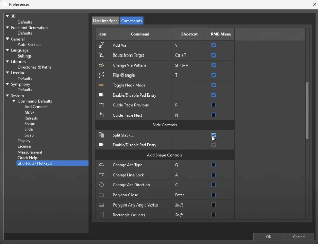
Enabling Slide Controls within the OrCAD X Preferences GUI for Splitting Stacks
Fundamentals of Routing High-Speed Signals
-Routing high-speed signals demands attention to a variety of aspects in order to ensure signal integrity and performance. Below, we delve into key technical considerations.
Signal Integrity Considerations
Impedance mismatches can cause signal reflections, leading to data corruption. Ensuring that trace impedance matches the source and load impedances is crucial. Controlled impedance traces are typically achieved by carefully selecting trace width, spacing, and the dielectric properties of the PCB material.-
Unwanted coupling between adjacent signal traces can induce crosstalk, degrading signal quality. To mitigate this, increasing the spacing between signal lines as much as routing restrictions allow is effective. Additionally, placing the conductor as close to the ground plane as possible couples the transmission line tightly to the ground plane and decouples it from adjacent signals.
Minimizing Electromagnetic Interference (EMI) and Noise
|
Method |
Description |
|
Differential Pair Routing |
For high-speed differential signals, such as LVDS or USB, routing the differential traces together (side-by-side) ensures any noise injection into the signal is a true common-mode noise, which gets rejected by the receiver. |
|
Ground Planes and Return Paths |
Routing high-speed signals over a solid ground plane is critical. A common ground plane below signal traces helps maintain signal integrity. |
|
Via Placement |
It is advisable to minimize the use of vias in high-speed signal paths, as each via introduces inductance and potential impedance discontinuities. To reduce their impact, ensure that vias are properly backdrilled or use blind/buried vias. |
Layer Stackup and Routing Strategies
A well-designed PCB stackup can significantly affect high-speed signal performance.
-
Implementing at least a four-layer PCB allows dedicating one of the inner layers to a full ground plane, which is beneficial for signal integrity.
-
Assigning high-speed signals to specific layers adjacent to continuous ground planes ensures a low-inductance return path, reducing EMI.
-
Avoid routing high-speed signals over splits in the reference plane or across different power domains, as this can cause impedance discontinuities and increased EMI.
Managing Timing and Skew
|
Method |
Description |
|
Matched-Length Routing |
Length tuning traces will ensure equal delays in high-speed interfaces, such as DDR memory buses. |
|
Propagation Delay and Trace Tuning |
Variations in trace lengths can lead to timing mismatches. Implementing serpentine traces (meanders) can help match trace lengths; however, it's crucial to maintain a minimum distance of four times the trace width between adjacent parts of the same trace to minimize crosstalk. |
|
Terminations and Signal Conditioning |
Proper termination resistors are essential to match the impedance of the transmission line, thereby minimizing reflections. Additionally, signal conditioning techniques, such as pre-emphasis or equalization, can enhance signal integrity over longer distances. |
Tips for Routing High-Speed Signals in OrCAD X
OrCAD X provides several routing tools to assist with high-speed signal design while ensuring adherence to constraints. The Add Connect command handles most routing tasks and includes manual and assisted modes to manage Design Rule Checks (DRCs) and optimize trace placement.
1. Using the Add Connect Command
-
Activating the Command: Select Add Connect from the floating toolbar. A helper window will appear, displaying adjustable routing properties. Users can toggle the window with the X hotkey.
-
Manual Routing: Designers can place traces without automatic assistance in manual mode. If a trace violates a design rule, it will flag a DRC error.
2. Controlling Trace Width and Behavior
-
Setting Trace Width: Width can be set using the dropdown menu or entered manually. There are three modes:
-
Auto: Uses predefined constraints based on routing start point.
-
Constraint Mode: Adheres to width values set in the Constraint Manager.
-
Neck Mode: Adjusts width for tighter routing in limited spaces.
-
Cornering and Line Behavior: Sliders can enable arc routing and free-angle corners to control routing paths.
3. Utilizing Clearance View for Spacing Constraints
-
Visualizing Routing Channels: Enabling clearance view highlights available routing paths by displaying bumpers around copper features based on spacing constraints.
-
Smoothing: A smoothing slider can be adjusted to reduce the number of trace vertices, simplifying routing paths.
4. Assisted Routing: Hug and Shove Modes
-
Hug Mode: Routes traces as close to existing copper features while maintaining spacing constraints. This mode is most effective when the clearance view is enabled.
-
Shove Mode: Moves existing traces and (optionally) vias to accommodate new routes without violating constraints. Users can enable via shoving by toggling a checkbox in the routing options.
-
Disabling Clearance View in Shove Mode: Since shove mode actively moves copper features, disabling clearance view prevents unnecessary visual clutter.
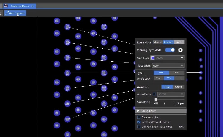
Add Connect Helper Window in OrCAD X
Cadence’s OrCAD X platform equips designers with specialized tools like the ‘Add Connect’ command and advanced via management features to ensure precision when routing high-speed signals. Whether you're managing signal integrity, timing, or layer stack configurations, OrCAD X simplifies the process and ensures adherence to industry standards. Learn more about OrCAD X and discover how these tools can elevate your design.
Leading electronics providers rely on Cadence products to optimize power, space, and energy needs for a wide variety of market applications. To learn more about our innovative solutions, subscribe to our newsletter or our YouTube channel.