Rigid-Flex PCB Design Guidelines
Key Takeaways
-
Avoid plated through holes in bending areas, use teardrops and anchors for connecting traces, and maintain straight, perpendicular traces across flex zones.
-
Use cross-hatched ground planes in flexible areas to maintain flexibility and reduce stress on the copper.
-
Utilize PCB design software like OrCAD X for rigid-flex designs, offering features like zone-specific stack-ups, real-time DRC updates, and advanced 3D visualization.
A rigid-flex PCB is space-saving and shock-resistant
A rigid-flex PCB is a PCB that combines both elements of a hardboard and a flexible PCB in a single piece. A rigid-flex design is typically made up of two or more rigid areas that are interconnected by a flexible strip. The synergistic property of the rigid and flex elements allow the PCB to be bent or folded in applications.
A rigid-flex design eliminates the need for connectors and interconnecting cables. Rigid-flex PCBs are also easier to install, as the entire design is manufactured on a single PCB. Rigid-flex PCBs, while offering substantial benefits, are a bit more complex to design than standard FR4 boards, necessitating adherence to specific rigid-flex PCB design guidelines to ensure optimal performance and reliability.
Rigid Flex PCB Design Guidelines
|
Guideline Category |
Details |
|
Material Considerations |
|
|
Use of Corners and Teardrops |
|
|
Plated Through Holes and Bending Areas |
|
|
Routing Across Bending Area |
|
|
Ground Plane Considerations |
|
|
|
|
Design Software Utilization |
|
Material Considerations for Rigid-Flex PCB Design
You should consult your PCB manufacturer before starting a design. Depending on whether the PCB is meant for dynamic or stable bend, the choice of copper type, the number of layers, bend radius, and coverlays may differ.
A dynamic bend rigid-flex PCB is installed in an environment where it will constantly be subjected to bending. Therefore, it is recommended to use no more than 2 layers and ensure that the bend radius is at least 100 times the material thickness.
Meanwhile, it’s possible to have up to 10 to 20 layers for a rigid-flex PCB that’s meant for stable-bend installations. It is not subjected to repeated bending force and that means a smaller bending radius of about 10 times its material thickness is also possible.
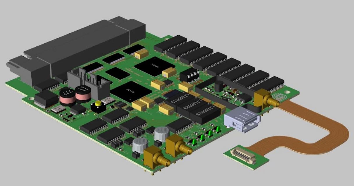
PCB Designed in OrCAD X With a Flexible Connector
Important Rigid-Flex PCB Design Guidelines
For all the advantages of rigid-flex PCBs, they also present challenges for PCB designers. Designers must consider not only the electrical aspects of a design but also the mechanical dynamics of the PCB. If you happen to be working on a rigid-flex PCB, following rigid-flex PCB design guidelines will save you from committing costly mistakes.
Avoid Plated Through Holes on the Bending Areas
Avoid placing pads and vias on the bending area of the flex part of a PCB. Areas near the bend line will deliver mechanical stress that could jeopardize the structure of the plated holes.
Pads and vias can be placed on areas that are not subjected to bending, although it’s not recommended. In such cases, use anchors to strengthen the plated holes. Additionally, use a teardrop to connect the trace to the plated hole for stronger joints. It’s also a good practice to use larger pads and vias.
Pay Attention to Routing Across the Bend Area
Traces across the bend line should be kept straight and perpendicular. It’s better to use narrower traces spread evenly across the flexible area. Adding dummy traces can help increase mechanical sturdiness, protecting the traces from breaking. For a double-layer design, traces should be routed alternately on both the top and bottom layers.
Avoid making any corners with the traces on the bending area. If the traces need to change direction on a flex PCB, use curves rather than sharp 45° or 90° corners.
Use a Cross-Hatched Ground Plane
If you’re pouring the ground plane as a solid area of copper, you’ll risk putting a lot of stress on it and reducing its flexibility. Instead, use a cross-hatched ground plane on the flex area of the PCB.
It goes without saying that using a PCB design software that supports rigid-flex PCB design guidelines helps in creating an error-free prototype. OrCAD X enables stack-up by zones and inter-layer checks, which are handy in rigid-flex design.
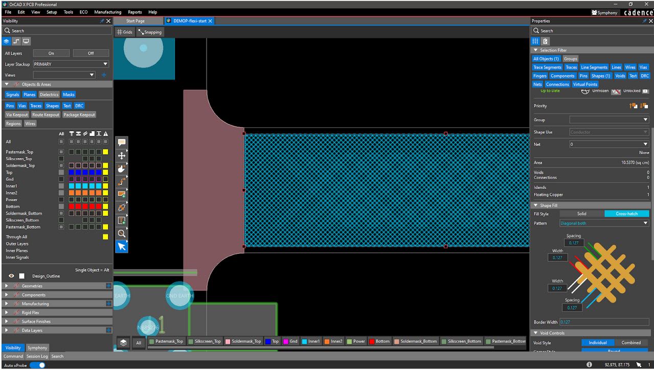
Cross-hatch pattern on a flex region of a PCB in OrCAD X
How OrCAD X Ensures Adherence to Rigid Flex PCB Design Guidelines
|
Guideline |
OrCAD X Feature |
|
Plated Through Holes and Bending Areas |
Constraint Manager can be used to set rules for avoiding plated through holes in bending areas and proper via placement. |
|
Design for Manufacturing (DFM) Checks |
DFM wizard and real-time DRC updates to ensure manufacturing constraints are met throughout the design process. |
|
Advanced 3D engine to visualize and verify rigid-flex designs, detect collisions, and optimize assembly in tight enclosures. |
|
|
This integration enables better coordination between mechanical and electronic design teams, crucial for high-reliability needs in various industries. It helps ensure that the PCB design meets mechanical constraints and operational requirements, reducing rework and ensuring reliability. |
|
|
Impedance Workflow |
Impedance analysis tools to ensure signal integrity across flexible and rigid sections of the PCB. |
|
The ability to clearly define and configure cross-sections for different zones of the PCB (rigid and flex) is required for applications involving flexible connections and flex-to-install scenarios. This feature ensures that different parts of the PCB behave as expected under operational conditions. |
|
|
Manipulation According to Material Flexure and Bend Radii |
OrCAD X allows designers to adjust 3D assemblies based on material flexibility and bend radii. This capability is specifically valuable for dynamic flexing applications. |
|
Interactive 3D Adjustments and Collision Detection |
Being able to adjust designs in real-time and check for collisions in a 3D space helps designers optimize layouts for all applications mentioned. This is especially beneficial in dense packaging, where space is at a premium and all components must fit precisely. |
|
Export 3D Data for External Analysis |
The capability to export 3D data for further analysis helps in the verification and validation process (which is crucial for all applications) to ensure designs meet the necessary standards and functionalities before going into production. |
To explore how OrCAD X can ensure you follow rigid flex PCB design guidelines, visit our PCB Design and Analysis Software page. Discover the robust capabilities of OrCAD X and take your rigid-flex PCB designs to the next level.