Understanding PCB Ground Plane Capacitance
Key Takeaways
-
The ground plane serves as a zero-volt return path in PCBs, which is crucial for reducing electrical noise by using capacitance to stabilize voltage fluctuations.
-
Different applications require specific capacitance ranges, from 200 picofarads for small pulses to 1 nanofarad for larger fluctuations.
-
OrCAD X offers tools like Copper Shapes Tool and Z Copy Method to aid designers in effectively managing ground plane capacitance.
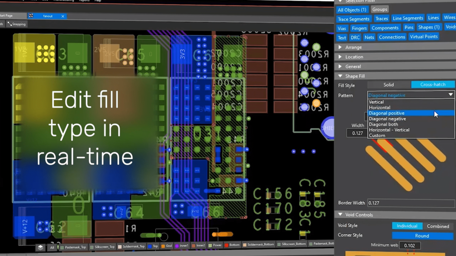
OrCAD X shape fill features shown on the green lattice fill.
Ground serves as the return path at zero volts for power planes in a PCB. Capacitance is useful between power and ground planes due to electrical noise interference. Rapid voltage transitions in chips or transistors induce reflections and noise spikes in power traces, along with quick voltage rises that drive signals into low impedance, causing initial dips and subsequent spikes in power lines. To solve this, capacitors absorb and mitigate these electrical voltage variations to eliminate noise.
Factors Affecting Ground-Power Plane Capacitance
|
Factor |
Description |
How to Adjust/Set |
|
Layer Distance |
The distance between power and ground planes affects capacitance. |
Minimize the distance by specifying thinner dielectric layers (prepreg) between the planes. |
|
Dielectric Material |
The type of dielectric material used between planes influences the capacitance. |
Choose materials with higher dielectric constants, like specific epoxy resin or fiberglass types. |
|
Copper Area |
The surface area of the copper planes impacts the capacitance value. |
Maximize the overlap area of power and ground planes to increase capacitance. |
|
Copper Thickness |
The thickness of the copper layers can have a secondary effect on capacitance. |
Use standard copper thickness (e.g., 1 oz/ft²) as thickness has minimal impact on capacitance. |
|
Stack-Up Configuration |
This refers to the overall arrangement of layers and materials in the PCB. The distance between the copper layers affects capacitance. |
Customize the stack-up to have power and ground planes closer together, ideally in the middle layers. More expensive, custom boards can specify thinner dielectric layers to enhance capacitance. |
|
Power/Ground Plane Capacitance |
Capacitance between power and ground planes helps supply rapid switching currents and reduce EMI. |
Keep power and ground planes close (less than 3 mils apart) for effective interplane capacitance. A larger gap reduces capacitance, while closer layers increase it. While not replacing discrete capacitors, closely spaced planes reduce loop inductance and enhance overall board performance. |
|
Plane Inductance Spread |
Ground and power planes have inductance spreading, which makes them less effective as point-specific bypass capacitors. |
Minimize plane size or use additional discrete capacitors in specific locations to supplement interplane capacitance. |
What Electronically Happens During a Voltage Dip?
When a signal rises rapidly due to a sudden draw by a load, it can cause a dip in the power line. Subsequently, the power supply circuitry attempts to correct this by shooting the voltage back up, potentially causing it to spike over the desired nominal voltage, thus generating more electrical noise. As a lot of power circuitry uses a feedback loop, even if extremely optimized, it will take time to correct and stabilize the voltage, making these spikes almost inevitable.
The Solution to Voltage Spikes Through Ground Plane Capacitance
Capacitors can absorb the initial dip and subsequent spike in the power line, maintaining its stability. Depending on the frequency of the spike, several sized capacitors can be used:
-
Small-capacity capacitors are suitable for higher-frequency, smaller pulses within the 200 to 1000 picofarad range.
-
For larger bumps, capacitors sized between 0.1 and 1 nanofarads can be utilized.
However, instead of dispersing numerous capacitors across the entire board, it is beneficial to have a built-in capacitance between the ground plane and the power plane.
Interplane capacitance is essential in modern logic circuits to maintain a steady supply to cores. A discrete capacitor on power rails fails with high-frequency signals due to inductance. Instead, the close proximity of power and ground planes ensures interplane capacitance, stabilizing power distribution and reducing EMI failures and voltage fluctuations.

Diagram illustrating PCB ground/power plane capacitance
Power Plane Capacitance
For high-frequency applications, decoupling using discrete capacitors becomes less effective, necessitating the utilization of power plane capacitance to mitigate noise at these frequencies. The concept of plane capacitance can be grasped by examining the classic parallel plate capacitor, where the electric field generated between a power plane and a ground plane results in capacitance. The magnitude of this capacitance is determined by the equation:
Cplane = (ε0εrA) / t
Where:
-
εο represents the permittivity of free space
-
εr is the relative permittivity of the dielectric used
-
A denotes the area of overlap
-
t is the thickness of the FR4 dielectric (or other material), the separation between the plates
In cases where ground planes are on both sides of the power island, the capacitance must be calculated for each side and summed to determine the total capacitance. Plane capacitance is the primary method of decoupling at high frequencies and should thus be an integral consideration in any high-speed design, as discrete capacitors prove less effective in such scenarios.
OrCAD X Tools for Managing Ground Plane Capacitance
|
Feature |
Functionality |
|
Copper Shapes Tool |
Guides users through creating ground planes using rectangular copper shapes, allowing the selection of specific nets and placement on designated layers, facilitating a robust connection path for ground nets. |
|
Grids and Snapping |
Enables precise component placement and alignment through toggleable grids and customizable snapping configurations. This is crucial for the accurate positioning of ground and power planes to ensure optimal layout and spacing. |
|
Merging Copper Shapes |
Enables the merging of polygonal shapes for power planes, applicable for creating complex plane configurations that ensure continuous power delivery and signal integrity across the board. |
|
Z Copy Method |
Utilizes the Z copy feature to duplicate shapes to different layers or with offsets, ideal for replicating ground or power plane designs across multiple layers or adjusting their placement while maintaining design integrity. |
|
Allows customization of how a shape/copper pour is filled – from solid, crosshatch, diagonal, and horizontal. Allows for fine-tuning copper areas affecting capacitance and thermal distribution. |
|
|
Shape Drawing Tools |
Allows easy drawing and editing of shapes similar to PowerPoint. Users can select types and properties of shapes, such as layers and nets, which is essential for defining ground planes directly on the PCB design canvas. |
|
2D and 3D Visualization |
Offers the ability to swap between 2D and 3D views and from various camera angles, enhancing the visualization of ground planes in relation to other board components. This helps in reviewing and verifying the layout before finalization. |
Sign up for a free trial of OrCAD X to experience firsthand how our advanced tools can help you expertly manage your PCB ground plane capacitance. Don't miss out—optimize your designs today!
Leading electronics providers rely on Cadence products to optimize power, space, and energy needs for a wide variety of market applications. To learn more about our innovative solutions, talk to our team of experts or subscribe to our YouTube channel.