Signal Integrity for High-Speed Design in PCB Layout
Key Takeaways
-
Signal integrity basics in printed circuit boards.
-
Layout recommendations for combating signal integrity problems in PCB designs.
-
PCB layout features, functions, and tools that will help you with good signal integrity in your design.
Crosstalk Checking in PCB Layout for Signal Integrity Validation
As circuit board signal speeds increase, so does the need to lay them out to achieve their best electrical performance. At one time, PCB layout engineers didn’t have to worry about how they routed their traces, as signal speeds were slow enough to not be affected by the physical layout. However, as signal speeds rose, the possibility of signal degradation due to poor high-speed layout practices increased. This degradation can create problems with circuit timing and signal amplitude levels, often resulting in the failure of the circuit due to misreading the signal states.
Therefore, the goal of a good PCB layout is to minimize the amount of signal degradation as much as possible. This can be done by carefully configuring the board layer stackup, the components’ placement, and the routing strategies used. When these tactics are used, designers can expect to achieve good signal integrity for high-speed design. Here are some of the basic principles of this type of layout.
The Basics of PCB Signal Integrity
Many interferences can degrade the purity of a signal in a printed circuit board, and the higher the signal speeds, the more they can be affected by these problems. These interferences include electromagnetic coupling or crosstalk, EMI, impedance mismatches, and ground bounce. If not controlled, these noises will degrade the fidelity of the signal to the point where it can suffer from transmission errors. Poor signal integrity can reveal itself in intermittent problems that are difficult to diagnose or outright system failure. Another potential problem is the difference between prototyping and production-built boards. If the signal integrity is barely marginal in the prototype, it may be completely unacceptable in a production unit.
It is incumbent on circuit board engineers to ensure their designs have good signal integrity. However, the difficulty that PCB designers face is that these interferences can influence each other, and correcting one problem can lead to others unexpectedly springing up. Designers need to remember that they will never get rid of all the signal integrity problems on a circuit board, as there will always be some level of noise or interference on the board. Instead, the designer’s goal should be to efficiently manage the interferences in the PCB layout to keep them under the allowable noise budget for the design. Let’s look at some specific areas of signal integrity problems on a circuit board and how you can control them with good PCB layout practices.
The key to a good PCB layout is careful consideration of signal integrity for high-speed design
Layout Recommendations for Signal Integrity in High-Speed Designs
Here are four of the main signal integrity problems that PCB layout designers need to be aware of and the design strategies that are useful for correcting them.
Unintentional Electromagnetic Coupling Between Traces
When a high-speed signal is routed too close to another, the stronger signal pulse may overpower the weaker signal. This crosstalk between signals can cause the weaker signal to mimic the stronger one instead of transmitting its intended pulse, resulting in miscommunication within the system. Not only can this happen to traces that are routed side-by-side, but also between layers of the board as well.
To prevent crosstalk, circuit board designers should consider the following steps in their layout:
- Configure the board layer stackup to position ground planes between layers containing sensitive routing of high-speed signals.
- It is also good to swap directions on each routing layer to minimize the chance of broadside coupling, which crosstalk between layers.
- Don’t run sensitive high-speed signals, such as clock lines, together in parallel for long distances.
- Use an increased amount of distance between high-speed traces. These sensitive nets will need more than the standard manufacturing distance between them to guard against crosstalk.
Electromagnetic Interference With Other Signals
Circuit boards that are not laid out correctly can radiate a lot of EMI. Long traces can behave as antennas, and trace stubs or unused via barrels can also emit EMI. One of the worst culprits for EMI is the lack of a clear signal return path for high-speed signals on the reference plane. The signal returns will wander around the board using whatever method possible to return and create a lot of noise and interference while doing so. EMI can harm other circuitry on the board or cause problems for nearby hardware.
To manage EMI in circuit board layouts, designers need to follow these basic rules:
- Route circuit board traces as short as possible.
- Confine high-speed sensitive signal routing to one board layer whenever possible.
- Place digital and analog components separate from each other in order to maintain isolation between the two.
- Above all, do not route high-speed signals across a split reference plane, as that will destroy its clear signal return path.
Changes in Impedance Values Within High-Speed Traces
For the best signal integrity in a high-speed trace, it must have both a consistent and uniform trace and a clear return path. We’ve already seen the importance of the signal return path on a reference plane, but maintaining the uniformity of the trace itself is just as essential. Uncontrolled traces can change their impedance values from one end of the line to the other depending on the conditions of the board where they are laid out. Without impedance control, high-speed signals may end up getting reflected back to their source when they enter a zone on the board where their trace changes in impedance value.
For successfully controlled impedance routing, the circuit board must be correctly configured according to calculations based on these guidelines:
- Controlled impedance routing needs to be confined to a layer that is adjacent to a reference plane.
- The vertical spacing between the controlled impedance traces and the adjacent reference plane must be included in the calculations.
- The dielectric constant (Dk) of the non-conductive circuit board material between the trace and the reference plane also needs to be part of the overall impedance controlled calculations.
- Finally, the impedance calculations will give you the correct trace width to work with to hold the impedance value that you need for your sensitive high-speed trace routing. The calculations also need to specify the thickness of the trace or the trace’s cross-section volume.
Simultaneous Switching Noise (SSN)
Not only do high-speed components switch between high and low states much faster than slower operating devices, but there are also typically more of them on a circuit board than there used to be. With so many devices rapidly switching states, the voltages may not return all the way back down to their reference ground level and instead “bounce” above it. If a low state voltage bounces above its ground level, the low state may be misinterpreted as a high state, instead resulting in false or double switching. This condition can potentially disrupt the normal operation of the circuits. Additionally, without the signal returning all the way down to its low state, there is an unexpected increase of current in the trace, which creates noise on that signal.
To stop simultaneous switching noise or ground bounce, here are some layout tactics that can help:
- Use enough capacitors to stabilize the voltage for each device and absorb the ground bounce.
- Place the decoupling capacitors for the device as close as possible to the power pin that they are assigned to. This will help contain the current spikes while the device is switching.
- Each ground pin on a device should have its own connection to the ground plane and not be chained together with other ground connections.
- The power and ground connections throughout the power delivery network (PDN) should have wide traces and vias to increase the flow of current and reduce the amount of inductance.
With these four problem areas of signal integrity identified, let’s look next at some features in your design tools that can help you improve signal integrity for high-speed designs.
The Impedance Checking in Cadence’s Allegro PCB Editor
Useful Layout Tool Features
Today, PCB design tools have many useful features and functions to help layout designers verify the signal integrity of their high-speed designs in real-time. This allows many of the noise problems to be resolved before building the first physical prototype of the board. Cadence’s Allegro PCB Editor is a good example of these signal integrity analysis tools:
-
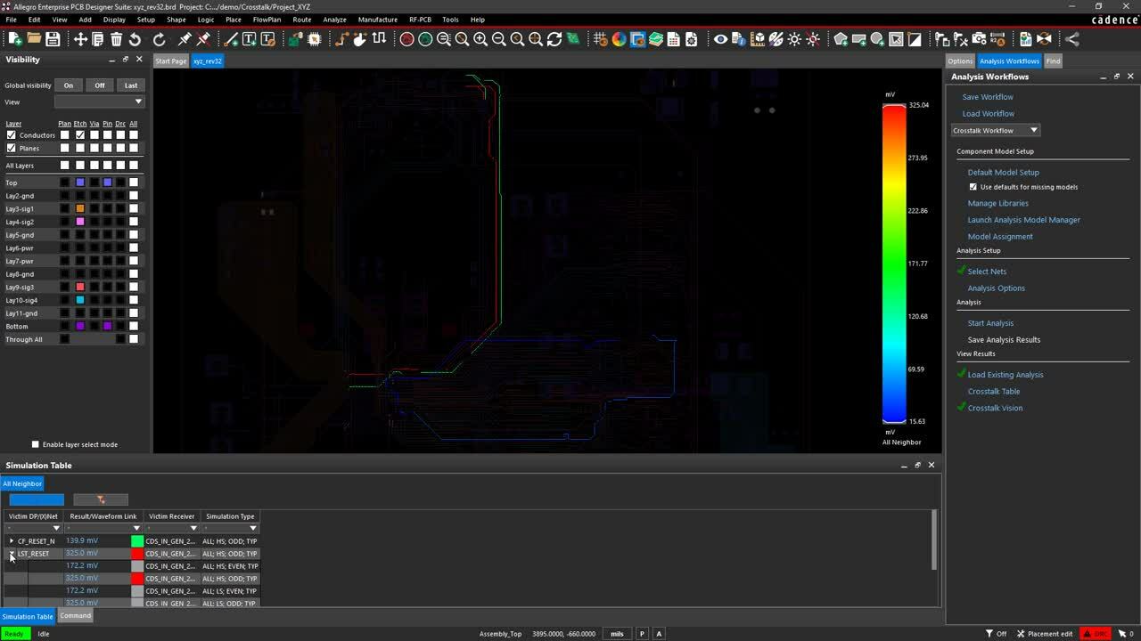
Crosstalk: Finding and correcting electromagnetic coupling problems has traditionally belonged to debugging the physical prototype of the board. This method of crosstalk detection usually required a lot of time and the use of specialized tools. However, with the crosstalk analysis tools built into the CAD system, layout designers can resolve most of these coupling issues before sending their designs out for manufacturing.
-
EMI: As we stated above, one of the main sources of EMI radiation on a circuit board is from poorly designed signal return paths. Even the best designers may not always spot areas of congestion on a ground plane that will disrupt the return path. Fortunately, the return path analysis tools in PCB layout CAD systems can easily find and report these problems to the designer.
-
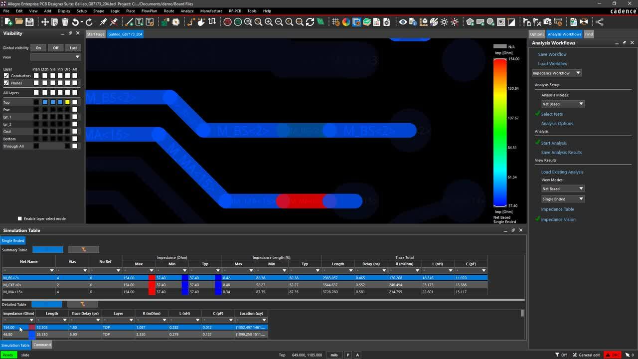
Impedance: For successful impedance-controlled routing, the circuit board needs to be set up with the correct board layer stackup, trace widths, and spacings. Most CAD systems provide an impedance calculator for this purpose, and Cadence goes a step further with the impedance analysis tools you can see in the image above. This gives the designer the ability to check in real-time whether or not the routing that they are laying out is actually holding the impedance values that are required. Additionally, the built-in reflection analysis tools will help the designer to spot potential areas of signal reflection due to impedance mismatches providing additional protection against signal integrity problems.
-
Power integrity: As we have seen, controlling ground bounce and other power integrity problems requires diligence in designing the PDN. Even one small problem, such as an inadequate amount of metal in a thermal connection, could be enough to create noise and degrade the power integrity of the board. With online tools like the IR drop analysis feature in Allegro, designers can quickly find problems with their PDN design and correct them.
These layout and post-layout analysis tools can be a real lifesaver for PCB designers and the high-speed designs they are creating. Another huge help is in laying out the board with the correct width and spacing values to begin with, and like with all these other helpful features, Allegro has that covered as well in their constraint manager.
Design rules for component placement are important for manufacturing and signal integrity
It All Starts in the Design Rules
Good signal integrity for high-speed design in a PCB layout starts with a well-developed set of design rules and constraints. If done correctly, these will govern trace width and spacing for different types of signals, including digital, analog, high-speed digital and analog, differential pairs, high-speed topologies, and, of course, the different power and ground requirements. They will also control routing layers, the routing direction on those layers, and special areas for necking down trace widths, such as within a BGA.
Design rules and constraints can also control how and where individual components or groups of components are placed. They can also be set up to catch potential fabrication and assembly problems, silkscreen errors, and many other issues that can delay or slow down the manufacturing of the circuit board.
For more information on high-speed design tactics, take a look at this E-book from Cadence.
If you’re looking to learn more about how Cadence has the solution for you, talk to our team of experts.