Rigid-Flex PCB Stackup Tools With OrCAD X
Key Takeaways
-
Rigid-flex stackups combine materials and processes from flex manufacturing with more traditional rigid boards.
-
Different rigid-flex structures are possible depending on how designers want to combine the discrete board types for the application.
-
The Cross-section Editor in OrCAD X helps design teams track and stay on top of complex multi-level stackups, including material data for more accurate simulations.
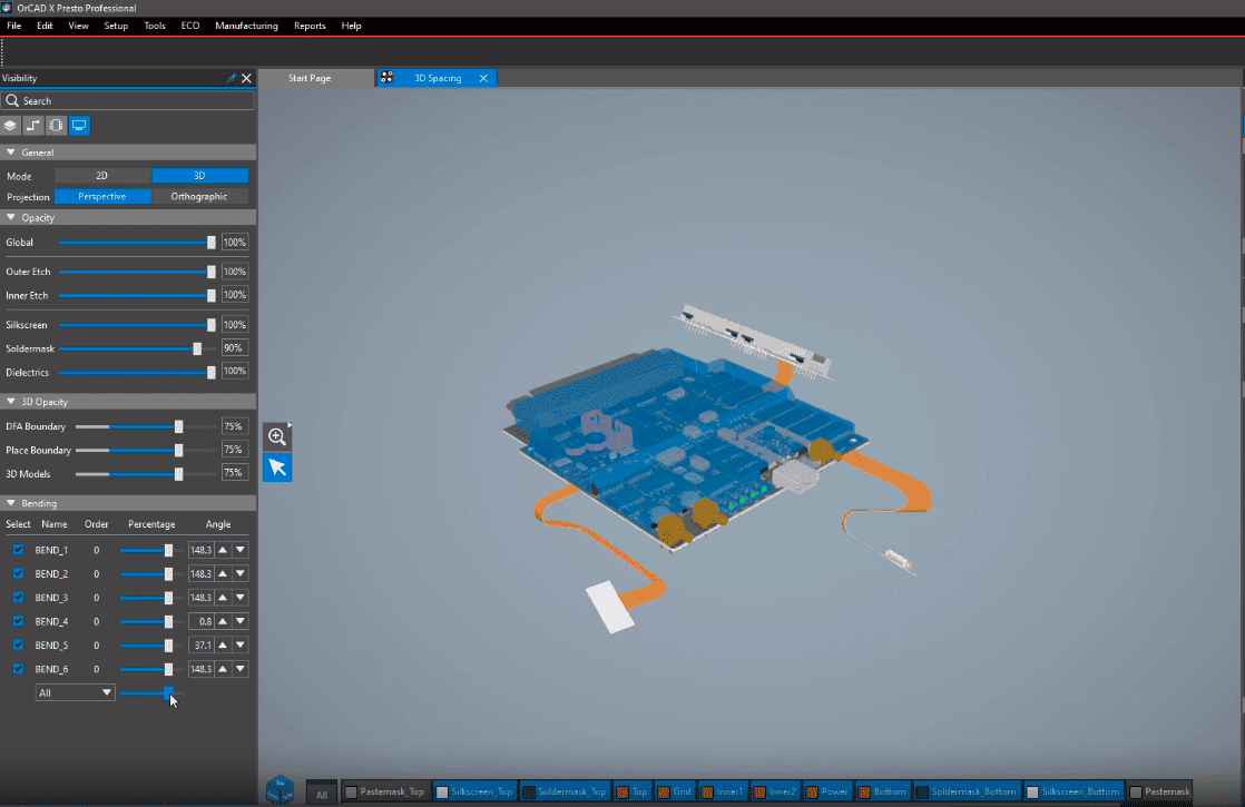
OrCAD X 3DX Canvas helps visualize rigid-flex PCB stackups with bend sliders.
Mounting needs for smaller form factor electronics have been the driving force for rigid-flex applications in recent years: one needs to look no further than their smartphone or laptop to see the flex circuits in action. When designing a flexible PCB, the designer must pair up the appropriate materials for the design and understand how these work into the flexible layer stackup. Rigid-flex PCB stackups must combine the application's mechanical constraints with the circuit's electrical considerations. In general, flex and rigid-flex manufacturing are more challenging for the manufacturer than standard rigid boards, which places a heavier burden on designers to optimize layout and stackup planning. OrCAD X gives designers a wealth of tools to navigate rigid-flex requirements for synergistic ECAD-MCAD integration.
Rigid Flex PCB Stackup Materials
|
Base flex |
Polyimide/polyamide provides mechanical flexure. Rigid-flex PCBs have an additional rigid region containing the polyimide as an inner layer (see below). |
|
Cu Conductor |
Copper conductor: Manufacturers prefer rolled-annealed copper foil to traditional electrodeposited copper foil. |
|
Coverlay |
The exposed copper circuitry of the flexible PCB uses a polyimide coverlay (sometimes called an “overlay”) material for protection. This material plays the same role as a solder mask in a rigid PCB (note that solder masking can offer additional environmental protection for some rigid-flex applications). |
|
Adhesive |
These epoxy-based materials bond the flex base material and coverlay onto the copper conductor. |
|
Stiffener |
These non-flexing regions of rigid-flex PCBs use FR4 or polyimide to provide rigidity. There are two methods for attaching stiffeners to the flex PCB: lamination or adhesion using a pressure-sensitive adhesive (PSA). |
Rigid-Flex PCB Stackup Breakdown
Many different layer stack configurations are possible in a flexible PCB or a rigid-flex PCB. The most basic uses a single flex region with two copper layers built on a flexible substrate material (polyimide), as shown below. This flex region can integrate into a rigid-flex PCB stackup or function independently; in a rigid-flex PCB, the coverlay film bonds to the prepreg during lamination to assemble the FR4 stiffener region on the flex ribbon..
A rigid-flex board with six rigid layers and two flex layers.
The rigid-flex stack-up typically comprises at least one flexible layer pair between rigid sections. The most commonly designed rigid-flex boards usually have double-sided flexible PCB laminated with rigid sections with prepreg layers, as shown in the figure above. Note that the stiffener sections use a prepreg to bond to the flex section in each arrangement. However, the layer stack shown above does not need to be limited to a single internal copper layer and two rigid FR4 layers. Multiple rigid layers can stack on each side of the flex region. Also, the FR4 layers on each end can have different layer counts, as these have individual lamination processes before the final lamination.
Multilayer Flex PCB Stackup
Two flexible layer pairs are usually not stacked on each other when the flex ribbon acts solely as an integrated connector. However, multiple coverlay-substrate layers can be laminated in succession to give a multilayer flex PCB.
A flex stackup of four layers. Odd layer counts are also viable through etching.
Bookbinder Rigid-Flex PCB Stackup
It’s also possible to have multiple rigid layers between stacked flex regions in a bookbinder-type flex stackup. In this stackup, the flexible layer pairs are stacked on top of each other with some prepreg, creating space between the flex ribbons. Ribbon bend radii closer to the inside of the bend must be shorter than ribbons closer to the outside.
Bookbinder rigid-flex stackup.
Due to the diverse range of options in building flex PCB layer stackups, designers should contact their fabrication house to collaborate on the stackup ASAP. Flex and rigid-flex PCBs offer many unique design approaches, but designers should check to ensure their idealized stackup (and design rules) reflect practical manufacturing tolerances.
Cadence Simplifies Complex Stackup Challenges
Rigid-flex PCB stackups need tools to manage material layer assignments; with the Cross-section Editor, OrCAD X users can create concurrent stackups to account for the difference in materials and processing across a rigid-flex PCB. Customization and view options also provide a quick visual representation of the stackup data table, supporting import/export options for IPC-2581 files. For all MCAD-ECAD integrated systems, the new OrCAD X platform puts the user experience at the forefront without sacrificing capabilities. Additionally, Cross-section Editor features like the Fill-In Material column enhance accuracy in supporting PCB Design and Analysis Software.
Leading electronics providers rely on Cadence products to optimize power, space, and energy needs for a wide variety of market applications. To learn more about our innovative solutions, talk to our team of experts or subscribe to our YouTube channel.