Taking a Circuit Board through OrCAD Layout for the First Time
Key Takeaways
-
Preparing your PCB design for layout.
-
Component placement and trace routing in OrCAD Layout.
-
Finalizing the design and creating manufacturing files.
Starting a layout in OrCAD PCB Designer.
As they say, there’s a first time for everything. Traditionally this phrase is reserved for momentous occasions such as skydiving or getting married, both of which involve taking a giant step into the unknown. But that phrase also works for other events in our lives that we are new to, like the first time an engineer uses OrCAD Layout for designing a printed circuit board.
If this phrase applies and you are about to open up a PCB design to be laid out in OrCAD for the first time, congratulations. You are about to embark on a journey of using one of the most advanced pieces of circuit board design software there is, enabling your productivity as a designer to grow exponentially. As with any new software, though, there are bound to be some questions as you dive into it. You may already be familiar with PCB layout on other systems, and you may have some experience in using OrCAD to capture schematics. But if you are new to Cadence’s OrCAD Layout software, this will give you a snapshot of what you can expect the first time that you use it.
Preparing and Setting up Your Design for OrCAD Layout
To begin a circuit board layout using OrCAD PCB Designer, you will first start with the schematic. The components in the schematic will need to have PCB footprints assigned to them before you can start your layout. To do this, you will open up the property editor for the schematic and enter the PCB footprint names for each component. This will require that those footprints are available for the layout database or they will have to be built and installed in the layout libraries. Another alternative, however, is to use the Search Provider tool in OrCAD Capture to pull in symbols, footprints, datasheets, and STEP models from a third-party provider.
The next step will be to transition the schematic connectivity data over to the layout in a process called netlisting. OrCAD gives you different options and configurations to tailor the two databases to each other, and when completed, the netlist data files will be in the PCB layout container. Now, you are ready to open the layout in OrCAD PCB Designer.
The first thing to do in the PCB editor is to set up the different design parameters available to you. OrCAD gives you many options to customize the environment to your specific needs and tastes. For instance, you can see in the picture below how OrCAD can be set up to either show or not show the net names on design objects in the display. Other parameters that can be adjusted include colors, units, text, grids, and other display preferences.
The display of net names on design objects being toggled on and off in OrCAD Layout.
The last part of setting up the design for layout is to create its physical characteristics starting with the board outline. By using the graphical capabilities of OrCAD, the board outline is created along with any special features that are required. This can be done by specifying the coordinates of the shape and letting the system create it for you or by manually drawing it in yourself. From there, you will use the Cross Section Editor to create the board layer stackup. Here you can specify materials and thicknesses of the conductor and dielectric layers of the board.
Finally, you will use the constraint manager to input all of your design rules and constraints. OrCAD also gives you the ability to import all of this data as well so that you can leverage work done in other systems or by your vendors. Once this is complete, you are ready to start placing components.
Placing Components and Other PCB Parts on the Board
The first part of placing components on the board is to work with the parts that are not included in the netlist. These include tooling and mounting holes or other mechanical parts that aren’t connected electrically. As you can see in the picture below, the placement tools are used to specify a mounting hole that the designer can locate either by entering the desired coordinates or placing it manually with the mouse.
A mounting hole being placed in a PCB design using OrCAD Layout.
Using the same placement functionality, the next step will be to place all of the electrical components on the board. As each component comes in, it can be rotated or mirrored to the other side of the board. The designer also has the same features available to edit components that are already placed on the board. There is another feature that is especially useful and that is to set up the schematic for cross-probing with the layout. This way you can select the parts you want to place in the schematic and they will activate for placement over in the layout. Once all of the components are placed on the board, you will be ready to move on to routing.
Connecting the Nets with PCB Trace Routing and Planes
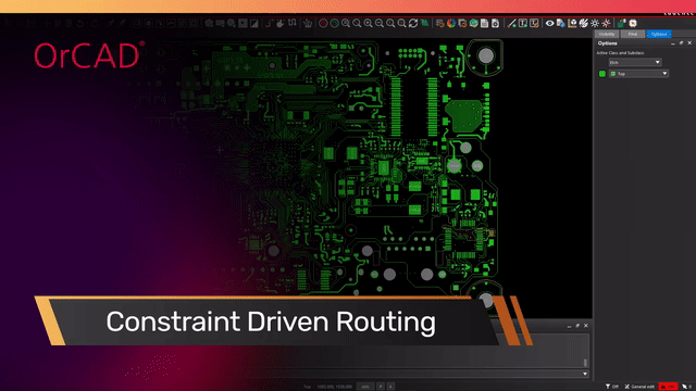
When it comes to connecting nets by routing traces, OrCAD PCB Designer gives you plenty of capabilities to work with. You can go into the manual routing mode and grab a guide (net) and route it as a trace. While routing the trace you can maneuver it around, pushing and shoving other traces out of the way. You can also select a previously routed trace and use the slide command to move it around, pushing and shoving other traces out of the way. It is here that the importance of setting up your design rules and constraints becomes evident as you work with the different trace widths, spacings, and vias of the nets to complete your routing as desired.
OrCAD also has multiple auto-routers built into it for different routing scenarios. The routers can be used for via fanout routing, clean-up passes, individual net routing, and full batch auto-routing. Once again, the design rules and constraints come into play as the routers will work with the different net classifications that you have set up in order to prioritize the connections.
Another useful tool in OrCAD’s trace routing arsenal is the ability to auto-interactively route traces on the board. While auto-routers will route all or part of the nets on your board according to the rules that have been set up, an auto-interactive router will combine its routing engine with the skill of the designer. The designer will specify the nets that are to be routed and then map out a path for the traces to follow. Once the desired direction is set and all of the pin swapping has been completed to make the routing path clean, the auto-routing engine will take over and route the traces in. This combination of human and machine interaction can give precision manual routing results at the speed of an auto-router.
An internal trace routing layer and a ground plane in a printed circuit board design.
Another part of routing is working with the power and ground nets in the design. While these can be easily routed with wider traces—thanks again to the specific design rules set up for them—they can also be routed on power and ground planes. OrCAD PCB Designer gives you plenty of options in the creation, configuration, and connectivity of metal plane layers. In the picture above, you can see the green ground plane with some thermal relief pads beneath the red routing layer. Not only does this give you an evenly distributed power distribution network, but it also helps to set up clean signal return paths for the trace routing.
The final part of routing a printed circuit board design is to check the integrity of the design work that has been done. With the design rules set up in the constraint manager, the online DRCs have already been guiding you as you place and route the board. However, at the end of the design, it is always a good practice to run one last check to make sure that the board is completely ready for manufacturing. OrCAD gives you 3D capabilities allowing you to check the board for clearance errors to mechanical objects, as well as helping to display the board for design reviews.
Completing the Layout and Releasing It for Manufacturing
Now that the board is fully placed, routed, and checked, it is time to get it ready for manufacturing. Again, OrCAD PCB Designer has a lot of features here to help you. First, you will want to clean up the board and finalize the silkscreen with OrCAD’s graphical editing tools. Next, you will need to create your manufacturing drawings by importing drawing pieces into the design, dimensioning them, and placing them all against a drawing format. Testpoints and other manufacturing features can all be added with the specific functionality in the tools designed for that.
At this point, the design is completed and is ready to be sent out for manufacturing. OrCAD gives you a lot of different tools to create and bundle together the different fabrication and assembly files required by a manufacturer, and there is another option available to you here as well. You can use the IPC-2581 export functionality to create a fully-contained manufacturing database that can be sent directly to your vendors. This format gives you the ability to exchange information back and forth with your manufacturers in order to ensure complete design integrity and containment.
With the power of OrCAD PCB Designer, you can create many different intricate PCB designs.
There is a lot to laying out a printed circuit board in order to create a design that can both perform as specified and be easily manufactured without any errors. With OrCAD PCB Designer, you have a CAD tool that is made specifically for this task with all of the latest design innovations built into it for success. To learn more about the overall PCB design process, take a look at this E-book.
If you’re looking to learn more about how Cadence has the solution for you, talk to us and our team of experts.