
Controlled Impedance Design Guide

Key Takeaways

  • Effective controlled impedance design involves managing factors such as trace width, copper thickness, dielectric thickness, and stack-up configuration to achieve specific impedance targets.

  • Differential pairs must be symmetrically routed with consistent spacing to maintain their impedance, with special care to avoid discontinuities caused by components or vias.

  • OrCAD X simplifies controlled impedance design by integrating analysis tools that automatically adjust trace parameters based on specified impedance values, helping ensure signal integrity and reliable performance.

Use OrCAD X for impedance analysis of all nets in the design.

Use OrCAD X for impedance analysis of all nets in the design.

Controlled impedance refers to the management of the characteristic impedance of a PCB transmission line formed by traces and their associated reference planes, essential for maintaining signal integrity at high frequencies by preventing signal distortion. It is determined by the physical dimensions and dielectric materials of the PCB and is measured in ohms (Ω). Read on as we discuss tips in this controlled impedance design guide.

Common PCB transmission lines requiring controlled impedance include single-ended microstrip, single-ended stripline, microstrip differential pair, stripline differential pair, embedded microstrip, and coplanar lines (both single-ended and differential). Achieving controlled impedance involves matching substrate material properties with trace dimensions to ensure the impedance remains constant along the entire PCB path—from source to destination—regardless of trace routing or layer changes.

When You Need Controlled Impedance

Controlled impedance is essential for PCBs in high-speed digital applications, like RF communication, telecommunications, computing with signal frequencies above 100MHz, and high-speed signal processing in systems like DDR, HDMI, and Ethernet.

Single-Ended vs. Differential Trace Impedance

It’s important to differentiate between these two types. Single-ended signals, such as those in parallel RGB LCD or camera interfaces, require routing with a specified single-ended impedance, which measures the impedance between the trace and its reference ground. In contrast, differential pair signals, like SATA, PCIe, HDMI, and USB, must be routed with differential impedance.

Controlled Impedance Design Guide: Board Parameters to Tune

Category

Details

Stack-Up Design

- The designer must develop the board's stack-up and calculate trace values for differential pairs and single-ended nets.
- Tasks can be performed by the designer or outsourced to fabrication partners.
- Key information required includes:
- Number of board layers
- Layers designated for routing controlled impedance traces
- Reference layers to be used
- PCB materials and copper thicknesses used in each layer
- Dielectric constant and dielectric height (e.g., 4 mils for inner layers and 3 mils for outer layers).

Trace Width

- Width of the copper foil on a PCB and its coating.
- Increased trace width leads to decreased impedance.
- Specified based on factors like required impedance during design.

Copper Thickness

- An increase in copper thickness leads to a decrease in impedance.

Dielectric Properties

- Increase in dielectric thickness usually results in modest increases in impedance.
- Significant reduction in impedance requires a considerable decrease in the insulating material's thickness.

Dielectric Constant

- Ratio of the electric permittivity of a material to that of a vacuum.
- Low, stable dielectric constants are suitable for high frequencies and controlled impedance.

Other Trace Configuration Impedance Factors

- Trace configuration (microstrip, stripline, differential pair).
- Proximity to ground or power planes.
- Trace spacing in differential pairs.
- Achieving controlled impedance is critical for high-frequency signal integrity in applications like telecommunications, video, and high-speed digital processing.

Planning and Specification Steps for Controlled Impedance

Design Aspect

Key Points

Specifying Layers and Target Impedance

  • Specify Layers and Target Ohms: Clearly indicate the layers on which impedance-controlled traces are to be routed and their target impedance values (e.g., 50 Ω on Layer 3).
  • Communicate with Manufacturer: Provide this information to the manufacturer to ensure proper stack-up design and impedance control.

Controlled Dielectric Thickness

  • Designer Provides Stack-Up: The designer supplies the controlled dielectric stack-up specifications to the manufacturer.
  • Manufacturing Focus: Without specified impedance traces, the manufacturer builds the board within a ±10% tolerance of the specified dielectric thickness from layer to layer.

Impedance Control

  • Parameters Affecting Impedance: Impedance is controlled through dielectric thickness, trace width, and spacing.
  • Manufacturer Testing: The manufacturer performs tests using Time Domain Reflectometry (TDR) coupons to verify that the desired impedance is achieved.
  • Adjustments: Based on initial test results, adjustments are made to meet the designer’s needs, ensuring boards are manufactured within the specified tolerance.

Determining Which Signals Require Controlled Impedance

  • Engineer Specification: Electrical engineers specify the values and types of controlled impedance signals so the layout team knows which nets are single-ended or differential pairs.
  • Consult Datasheets: Datasheets often provide detailed guidelines for signal groups, impedance values, spacing regulations, and routing layers.

Annotating the Schematic with Impedance Requirements

  • Specify in Schematics: During schematic design, engineers specify controlled impedance signals and classify nets as differential pairs or single-ended.
  • Provide Layout Guidelines: Precise layout design guidelines for controlled impedance are documented in the schematic or a separate "Read Me" file for the layout designer.

Determining Trace Parameters for Controlled Impedance

  • Trace Characteristics: A PCB trace is characterized by its thickness, height above the reference plane, width, and the dielectric constant (Er) of the PCB material.
  • Design Considerations: Careful consideration of these parameters is essential when designing controlled impedance PCBs.
  • Specify to Manufacturer: Designers can specify the number of layers, impedance values on specific layers, and materials for PCB fabrication to the manufacturer.

Distinguishing Controlled Impedance Traces from Other Traces

  • Unique Trace Widths: To distinguish controlled impedance traces from standard traces, assign unique widths (e.g., 5.1 mils instead of 5 mils).
  • Facilitates Manufacturing: This differentiation helps the manufacturer identify and adjust controlled impedance traces as needed

Routing and Layout Practices for Controlled Impedances

Design Aspect

Key Points

Maintaining Symmetry in Differential Pair Routing

  • Consistent Geometry: Ensure both traces in a differential pair have identical widths and consistent spacing to maintain impedance.
  • Symmetrical Routing: Route differential pairs symmetrically and parallel to each other to prevent impedance discontinuities and signal integrity issues.

Adequate Spacing Between Traces and Components (3W and 2W Rule)

  • Reduce Crosstalk: Maintain a spacing of at least three times the trace width (3W) between high-speed signals and other traces; a minimum of 2W is acceptable in constrained areas.
  • Not for Differential Pair Spacing: The 3W/2W rule does not apply to the spacing within differential pairs but to other adjacent traces and components.

Placement of Components, Vias, and Coupling Capacitors

  • Avoid Between Differential Pairs: Do not place components or vias between the traces of a differential pair, as they create impedance discontinuities.
  • Symmetrical Component Placement: Place coupling capacitors symmetrically on both traces of a differential pair to minimize signal disruption.
  • Maintain Spacing: Keep at least 5W spacing between differential pairs and adjacent pairs, and a keep-out zone of 30 mils from other signals (50 mils for clocks or periodic signals).

Length Matching of Differential Pairs

  • Prevent Delay Skew: Closely match the lengths of differential pair traces to avoid unacceptable delay skew.
  • Use Serpentine Routing: Implement serpentine traces on the shorter trace to equalize lengths, placing them near the source of mismatch.
  • Segment Matching: When changing layers or routing around obstacles, match the lengths in each segment individually.

Reference Layers for Return Path of Controlled Impedance Signals

  • Continuous Reference Planes: High-speed signals require a continuous reference plane for the return path to prevent noise coupling and EMI issues.
  • Avoid Split Planes: Do not route high-speed signals over split planes; if unavoidable, route around splits or use stitching capacitors.
  • Maintain Ground Plane Width: Ensure the ground plane extends at least 3W on each side of the trace.

Adding Stitching Capacitors and Vias

  • When Crossing Reference Planes: If a signal must cross between different reference planes (e.g., ground to power), place stitching capacitors (10 nF to 100 nF) close to the signal path to maintain the return current.
  • Symmetrical Placement: For differential pairs, place stitching capacitors symmetrically relative to both traces.
  • Stitching Vias Near Layer Changes: Add stitching vias close to signal vias when changing layers to support return currents and minimize impedance discontinuities.

Managing Return Paths Over Split Planes

  • Use Stitching Capacitors and Vias: Place them near the signal path when routing over plane obstructions or slots to maintain a continuous return path.
  • Avoid Slots Under Traces: Prevent routing high-speed signals over slots or voids in the reference plane; if unavoidable, use stitching techniques to minimize issues.

Minimizing Via Usage in Differential Pairs

  • Reduce Impedance Discontinuities: Minimize the use of vias in differential pair routing to prevent signal reflections.
  • Symmetrical Vias: If vias are necessary, place them symmetrically on both traces of the differential pair.

Avoiding Routing Over Plane and PCB Borders

  • Stay Within Boundaries: Do not route high-speed signals near the edges of reference planes or PCBs to prevent unintended radiation and coupling effects.
  • Maintain Signal Integrity: Routing near borders can cause impedance changes and increase susceptibility to external interference.
OrCAD X shows you impedance values for individual traces that must be impedance controlled.

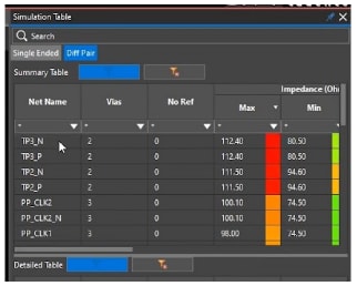
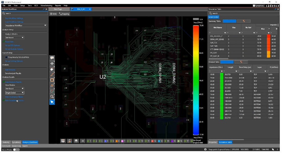
OrCAD X shows you impedance values (max and min) for individual traces.

Controlled Impedance Design With OrCAD X

Starting from release 24.1, OrCAD X integrates analysis tools directly into the design environment, streamlining controlled impedance design. You can perform both impedance and coupling analyses without external calculators or complex equations.

  • For impedance control, you access the Setup > Cross-section editor, where you can define your PCB's layer stackup, including layer thicknesses, dielectric constants, and reference planes.
  • By specifying your target single-ended or differential impedance values, OrCAD X automatically recalculates the necessary trace widths and spacing. For instance, setting a target single-ended impedance of 50 Ω will prompt OrCAD X to adjust the trace width accordingly, accounting for variations between outer and inner layers due to differing dielectric materials.

Impedance Design for Differential Pairs in OrCAD X

For differential pairs, you can define the coupling type—typically edge coupling—and set your desired differential impedance, (e.g.90 Ω for USB 3.0 applications). OrCAD X then asks whether to recalculate the line spacing or trace width based on your preference to maintain certain manufacturing constraints, like minimum trace widths to avoid extra fabrication costs. The software presents impedance results through color-coded overlays on your design and detailed tables showing minimum, maximum, and typical values for each net or segment, allowing you to quickly identify and address any mismatches.

OrCAD X also allows you to extract and model any net or differential pair into the Topology Explorer for advanced simulation and to enforce ideal interconnect constraints. This holistic approach empowers you to model different interconnect scenarios, simulate their performance, and apply constraints directly within your design environment. With OrCAD X's integrated analysis capabilities, you gain confidence that your PCB will meet controlled impedance requirements and function reliably in high-speed applications.

These integrated analysis tools help you follow the steps outlined in our controlled impedance design guide. To learn more, explore our PCB Design and Analysis Software and discover how OrCAD X can enhance your design workflow.

Leading electronics providers rely on Cadence products to optimize power, space, and energy needs for a wide variety of market applications. To learn more about our innovative solutions, talk to our team of experts or subscribe to our YouTube channel.