Home
Free Trial
Home
Free Trial
Read More
Content
Filter
10 results found
Featured
Reliability Overview | Allegro X
Featured
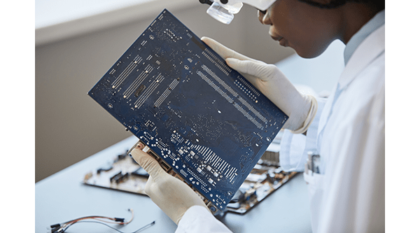
ICT vs Flying Probe: Factory Testing of PCB Assemblies
Featured
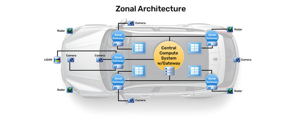
Software-Defined Vehicles: When Timing Becomes a Safety Risk
Featured
Reviewing The PCB Design Review Process
Featured
PCB Substrates Part 2: A Performance-Driven Approach to Reliability in 2025
Featured
PCB Design Strategies: Designing for High-Pin Count Devices
Featured
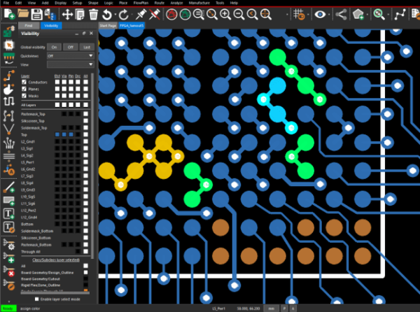
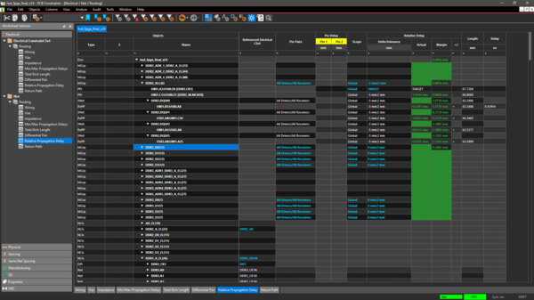
Constraint Driven Design in OrCAD X
Featured
Microvia Reliability in High-Density Designs
Featured
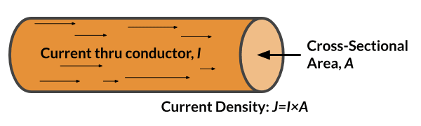
Copper Current Density in PCB Design
Featured
High Voltage PCB Design Guidelines
Featured
Products
None
Allegro X PCB
(2)
OrCAD X
(2)
Content types
None
Video
(1)
Blog
(9)
Solutions
None
Design for Reliability
(5)
PCB Layout
(6)
Simulation & Analysis
(1)
Constraint Management
(1)