Optimizing for PCB Trace Thickness vs Current Capacity
Key Takeaways
-
Trace width and copper layer thickness are crucial for managing the current-carrying capacity of PCBs, with standards provided by IPC-2152 and IPC-2221.
-
Location of a trace—external or internal—significantly affects its heat dissipation capabilities, influencing the choice of trace for safe temperature management.
-
Copper thickness is often measured in ounces per square foot, correlating directly to weight and providing a straightforward metric for determining necessary trace thickness.

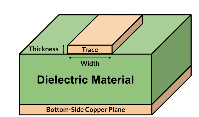
Diagram illustrating trace thickness and width
When designing PCBs, understanding the relationship between PCB trace thickness vs current capacity is crucial. The thickness of the trace directly influences how much current it can safely carry without overheating, making this a key factor in circuit design. By selecting the trace thickness based on expected current loads, engineers can ensure both the functionality and reliability of the PCB.
Considerations for Trace Thickness Selection
A PCB trace's ability to conduct current is governed by a set of factors, including its width, the copper's thickness, the maximum allowable temperature rise, its placement on the PCB, and whether a solder mask covers it. The task of selecting an appropriate trace width can be complex and is influenced by multiple considerations.
Summary of Considerations for Trace Thickness
|
Factor |
Description |
|
Trace's cross-sectional area |
Increases with higher power demands; greater areas are needed for wider traces. |
|
Trace's positioning |
Placement on top, bottom, or within inner layers influences heat dissipation capability. |
|
Trace's length |
Longer traces require careful consideration of width to maintain signal integrity and manage heat. |
|
Copper layer's thickness |
Directly measures trace thickness, with thicker copper needed for heavier currents. |
|
Trace's location |
Position on the board (external layers or internal) affects heat dissipation capabilities. |
To select the appropriate trace width for your PCB layout, you can consult a table that correlates trace width with current capacity. Alternatively, employing a calculator that adheres to either the IPC-2152 or IPC-2221 standards can provide precise guidance. Generally, the aim during operations is to maintain the temperature increase within the conductive paths of your board at a manageable 10-20 degrees Celsius.
IPC Regulations for Current Capacity
If you’d like especially detailed information, consider consulting one of the following IPC Regulations.
-
-
IPC-2152: This standard offers comprehensive guidance on the current-carrying capacity for PCBs, accommodating conditions like trace placement and copper thicknesses, and provides detailed models for assessing temperature rise.
-
IPC-2221: As a fundamental standard for PCB design, IPC-2221 sets forth the criteria for trace width related to current capacity and advises on a range of design factors, including electrical spacing and insulation, applicable across various applications.
-
Copper Thickness as a Measurement Unit
Copper thickness is often measured by weight per square foot; for example, when copper is described as 1oz, it means one square foot of copper weighs 1 ounce. Since the weight of copper is proportional to its thickness, the thickness can also be expressed in ounces. Additionally, these ounces can be converted into millimeters or mils.
-
- 0.5oz = 0.0007inch = 0.7mils = 0.018mm
- 1.0oz = 0.0014inch = 1.4mils = 0.035mm
- 2.0oz = 0.0034inch = 2.8mils = 0.070mm

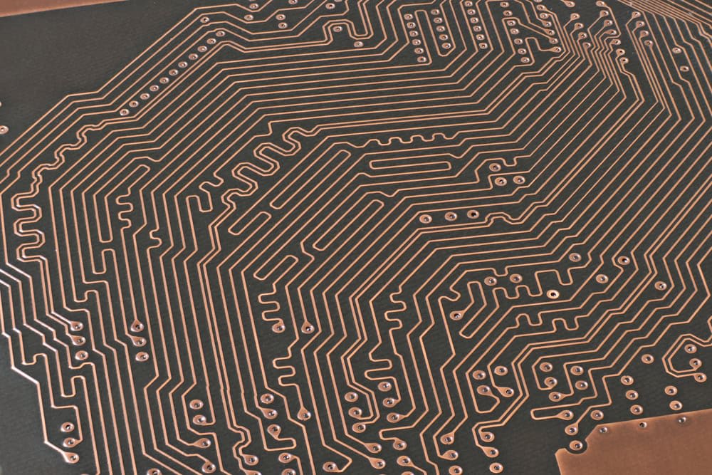
Traces on a printed circuit board (PCB)
Max Current Calculation Based on Thickness and Width
To calculate the maximum current capacity of a PCB trace, you can use the following formulas:
1. Cross-Sectional Area (A):
𝐴=𝑇×𝑊×1.378
Where:
-
- A is the cross-sectional area in square mils (𝑚𝑖𝑙s2)
- T is the trace thickness in ounces per square foot (𝑜𝑧/𝑓𝑡2)
- W is the trace width in mils (𝑚𝑖𝑙𝑠).
- The factor 1.378 converts the dimensions into the appropriate units (𝑚𝑖𝑙𝑠/𝑜𝑧/𝑓𝑡2).
2. Determining the Maximum Current (IMAX):
𝐼𝑀𝐴𝑋=(𝑘×𝑇𝑅𝐼𝑆𝐸𝑏)×𝐴
Where:
-
- IMAX is the maximum current in amperes (𝐴).
- TRISE is the maximum desired temperature rise in degrees Celsius (°𝐶).
- k = 0.048, b = 0.44, and c = 0.725 are constants specific to inner layer traces according to IPC-2221A Par. 6.2.
These formulas will help you estimate the maximum current a PCB trace can safely carry, considering its physical dimensions and the desired temperature limit.
Designing for High Current Parameters
To accommodate higher current requirements, the design approach involves the following information.
-
-
Applications requiring more substantial currents, such as motor controls that operate up to 50A, necessitate increased copper weights and broader trace widths. Widening the copper traces and augmenting their thickness to 2~4oz, also increases the spatial and layer requirements on the board.
-
Moreover, when a single-layer trace cannot support the required current, the trace can be extended across multiple layers with via stitching to link these layers, thereby enhancing the current-carrying capacity when the trace thickness remains constant across the layers. While using thicker copper traces of 2 oz or 3 oz increases the current capacity due to reduced resistivity, it also escalates the processing costs.
-
For high-power applications like electric automobiles and inverters, where currents exceed 100A, traditional copper traces are often inadequate. In such scenarios, copper bus bars, which are thicker than standard traces, can be employed. These busbars are soldered onto the PCB’s pads and are capable of handling high currents without overheating.
-
The table below specifies the maximum current carrying capacity for 2oz copper traces, allowing a temperature rise of 10°C. For other values, consider using a calculator.
Maximum Current Capacity for 2oz Copper Traces with Max Temp Rise of 10°C.
|
Maximum Current Capacity (Amps) |
Minimum Recommended Trace Width for Internal Layers (mil) |
Minimum Recommended Trace Width for External Layers (mil) |
|
2 |
20.03 |
19.95 |
|
4 |
66.86 |
66.59 |
|
6 |
135.34 |
134.78 |
|
8 |
223.21 |
222.28 |
|
10 |
329.05 |
327.68 |
When considering PCB trace thickness vs current for your designs, you can benefit from advanced PCB tools like OrCAD X. Its enhanced features help in PCB design, ensuring they meet the required specifications for current carrying capacity while avoiding overheating or functionality issues due to inadequate trace dimensions.
Leading electronics providers rely on Cadence products to optimize power, space, and energy needs for a wide variety of market applications. To learn more about our innovative solutions, talk to our team of experts or subscribe to our YouTube channel.