PCB Design Rules for Productivity and Profit
There are things you can do that don’t involve following rules. Walking down the street seems simple enough. Jaywalking is the first rule that comes to mind. You should be wearing some clothes while out in public. There are unwritten rules for walking as well. It would be nice if you stayed to the right or left according to the driving customs of your country. Bumping into others could end poorly. Even wearing the wrong color in some neighborhoods can be a problem. There are established rules that are codified in the Law Books and others that are just common sense.
PCB Design is kind of like that too. We have a book of rules just to keep aggressor nets away from victim nets. There may not be an explicit rule that requires an external oscillator right next to the relevant pins. It is normally left to the designer to incorporate the “tribal knowledge” that informs the placement. When it’s not possible to use an ideal location, then we must take additional care to isolate the XO lines within a guard band. Those rules and customs fit under the signal integrity umbrella.
Power is another branch altogether. Integrated circuits can require several different voltage domains. Even if two pins are using +3.3 volts, they may not want to be connected to the same voltage rail. They can be separated from each other with ferrite beads or, in many cases, a separate power supply.
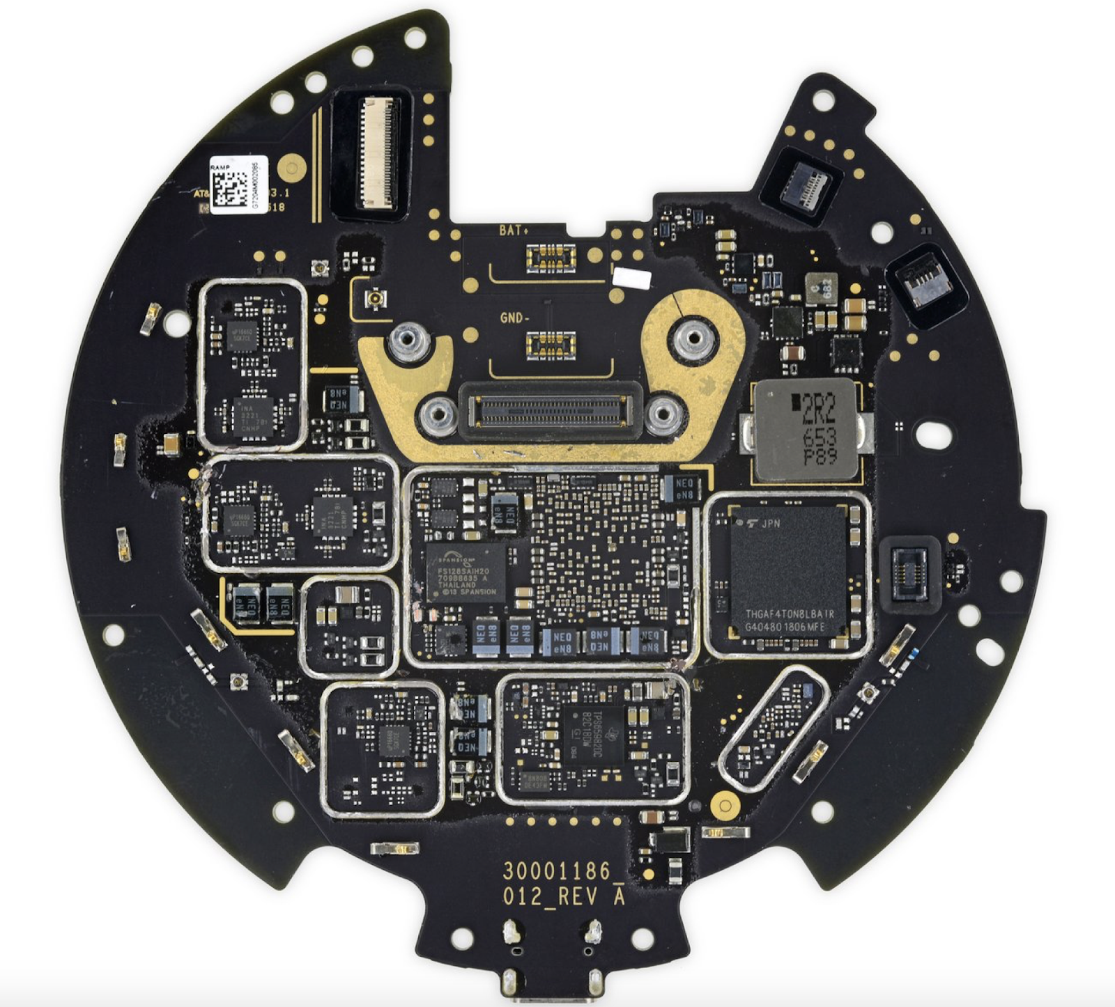
Image Credit: Ifixit - Tall fences make good neighbors and lots of shields make good coexistence on the PCB.
The voltage requirements of a complex chip can add up quickly. The requirements for several power domains can be met with a specific device that is made up of a bunch of individual power supplies that are tailored to the integrated circuit. Power Management Integrated Circuit (PMIC) is a class of devices with that function in mind. These devices have the noisy switching output pins around the perimeter and often end up with the external oscillator pins deep inside the BGA field. Add in all of those big inductors and you can see why seemingly suboptimal decisions may be required.
We get a data sheet with the requirements for the PMIC to power up the system on a chip (SOC). Those rules will be a test for the design rule checker. The connections are typically made with shapes spread over a few layers. We can assign line widths to the nets but it is more difficult when working with shapes that can be pierced by vias. A cluster of vias can create a slot in the shape that makes the effective width insufficient to cover the power requirements.
That is when the Power Integrity Engineer comes in. Feeding the boards power plane geometry into their special software will reveal any hot spots. Some domains may meet the requirement while others are in the red zone of the heat map. We may be able to add more copper but that usually comes at the expense of other shapes on the same layer. It can become a balancing act.
Getting all of the power planes to meet the spec in the simulation may take a few iterations. This is mostly evident with mobile electronics where board space and battery power are at a premium. Once the main device has a satisfactory set of shapes, the outlying devices remain spread out and they are usually handled with individual power supplies. We want those regulators placed close to the load.
Big inefficient linear regulators are getting to be like dinosaurs except for a few applications. Switch mode power supplies (SMPS) do the trick in most cases. The output on those devices have a lot of switching noise that is solved by placing a big inductor right next to the pin. We can establish a minimum trace width and a maximum trace length but again, the shapes that are often used are harder to constrain in that way. Consider the data sheet example as the design rule set. Even if it is not mentioned in the datasheet, the possibility to shield a device is often enough breathing room.
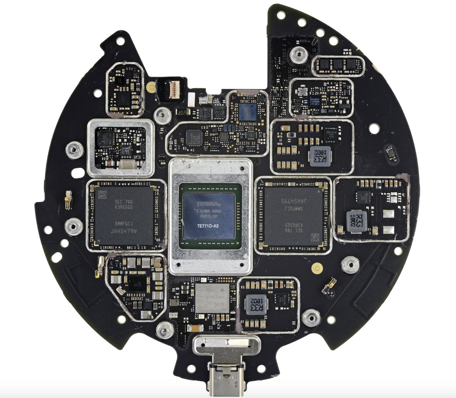
Image Credit: Ifixit - Shield rings are not always rectangular but the lower cost ones are.
For SMPS applications I would recommend a layout that is rectangular when all of the ancillary components are placed. Then a ring of ground should frame the power supply circuit. This is a way to add an optional EMI shield over the power supply if the layout fails the rules established by the Federal Communications Commision (FCC).
There are two basic rules that apply to electronic devices. The first and most obvious one is that the product cannot emit radiation that interferes with other nearby electronics. The corollary rule is that your gizmo should be immune to the ambient radiation from other devices. If it seems like wearing a belt AND suspenders, then you’re getting the point. It is hard to know where the failure will originate so caution is your guide.
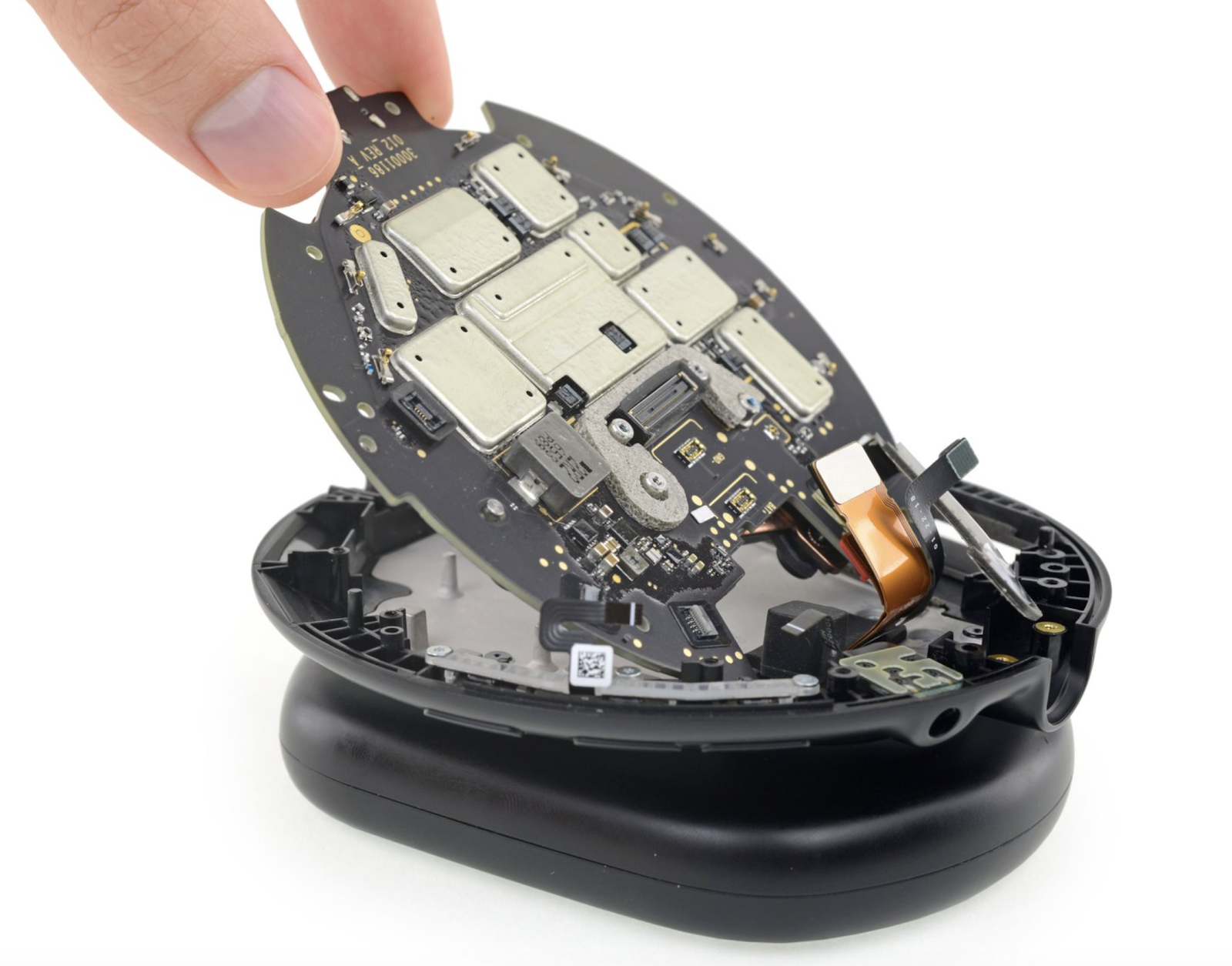
Image Credit: Ifixit - Modesty is the best policy when it comes to separating different circuits.
Ifixit is a website that does tear-downs of popular products. They ripped into a Magic Leap’s augmented reality reality goggles and it looked like every device on the main logic board lived in its own little metal capsule. This is an expensive way to definitively solve coexistence issues between all of the functions that have to happen in the AR/VR world.
Whether you are using the ECAD software to control line width, length and air gap or following the recommendations of the chip vendors for placement, there are rules that drive the layout to success. Incorporating all of those rules with another eye on Design for Fabrication, Assembly, and Test, (DFM, DFA & DFT) is not easy.
The newest versions of our layout software implement many new tools. Integrating SI/PI data is going to get us across the finish line sooner. Leaning on the baked in design rules helps navigate the most complex designs but also applies to the simpler boards as well. Planning for that up front is the ounce of prevention. Having to rework or redesign the PCB later on is the pound of cure. Go with prevention every time.