Why FOWLP Routing is Used in Advanced Packages
Heterogeneous integration is the primary approach to modern component design for many advanced applications. But with any new design modality comes bottlenecks that must be addressed. 3D-integrated heterogeneous components integrate multiple chiplets with diverse functions into a package, and these have to be linked together with conductive connections in the package. As the number of functions integrated into a package increases, one can see where the bottlenecks might arise in packaging design.
Today, interconnections in 3D heterogeneously integrated components use fanout wafer-level packaging (FOWLP) routing, which is an advancement over flip-chip BGA devices of the past. This approach to package routing was first used in mobile devices nearly a decade ago, but now it has found its way into high-performance computing and advanced processors in data center servers. For companies bringing their package and chip designs in-house, here is how this routing approach works and how packaging signal integrity ultimately converges to the PCB.
FOWLP Drives Heterogeneous Integration
Heterogeneously integrated packages have enabled the diverse functionality required in advanced components operating at the small-end of processing nodes. Packaging enabling integration of multiple dies has had to overcome both electrical and thermomechanical challenges. FOWLP packaging and routing has helped overcome the reliability challenges found in some 2.5D and 3D packages without compromising on routing.
FOWLP is also offered as a solution by TSMC, known as InFO packaging. The solution takes advantage of fab and packaging expertise by TSMC, whereas normally FOWLP would require packaging at an OSAT. FOWLP and InFO have been used in well-known instances:
-
2.5D packages integrating a memory die alongside the processor die
-
PoP for mobile devices, where a DRAM package was added on top of the main processor
-
InFO_oS 2.5D packaging allowing diverse dice (e.g., multiple logic dice) on the same substrate
These are just a few examples of the most widely produced integrated components with FOWLP. Although the industry is working towards high-volume 3D stacking of packages with TSVs, PoP in FOWLP (or InFO-PoP) provides a similar 3D stacking feature with interconnect routing in the redistribution layer (RDL).
PoP structure. [Source: TSMC]
Routing in the RDL extends beyond the primary logic die and is used to connect dice together, both vertically and horizontally. By extending the traces outward from the die, vertical routes and skip-layer routes in the substrate will enable a larger pin pitch on the package if needed. In general, the packaged footprint can be larger than the area occupied by the dice, but the packages can be quite thin and can have lower production costs.
The other important aspect of FOWLP routing is its heightened reliability. The reliability of these systems is greater than 3D stacked packages due to the extension of routing away from the die. This includes PoP in FOWLP due to the vertical via structures reaching the top package. Full package evaluation demands complex simulations that examine both the electrical behavior and device reliability.
Multiphysics Simulation Spans the Entire Interconnect
Reliability and electrical channel design are the two main factors to evaluate in multiphysics simulations for FOWLP. Channel design in terms of physical routing is straightforward, but via transitions are increasingly difficult to design due to the vias used in vertical transitions in FOWLP routing. Vias and pads are the major factors that will limit bandwidth at mmWave range frequencies in digital systems.
Standard electrical simulations will work for via and pad simulations, but a multiphysics approach is needed to understand reliability. Thermomechanical reliability is related to the packaging materials and construction, which is one of the reasons why FOWLP has been so successful for heterogeneously integrated components. Some of the main questions to answer in package thermomechanical simulations include:
-
Do the CTE values for the die, encapsulation, and substrate materials create excess strain?
-
Do the encapsulation materials enable high heat dissipation to the package exterior?
-
Will the substrate material minimize strain on the interconnects and dice?
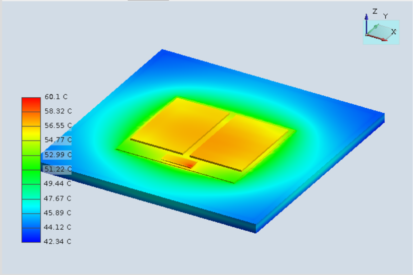
Thermal and mechanical co-simulation routines help to identify hot spots and excess strain in the component package.
(Alt Text: FOWLP routing)
Electronics design teams are becoming more multi-disciplined and will need to take the lead on packaging alongside PCB design in complex systems. No matter what you need to design, you can build it with the best set of PCB design features in Allegro X from Cadence. Only Cadence offers a comprehensive set of circuit, IC, and PCB design tools for any application and any level of complexity.
Subscribe to our newsletter for the latest updates. If you’re looking to learn more about how Cadence has the solution for you, talk to our team of experts.