The Next Generation of DDR5 Is Near: Here’s How to Prepare
This past summer, Cadence and Micron teamed up to demo the first IP interface in silicon for a preliminary version of the DDR5-4400 IMC. The chip was fabricated with TSMC’s 7nm Fin Field-Effect Transistor (FinFET) process, and boasts an impressive 4400 MT/s data rate.
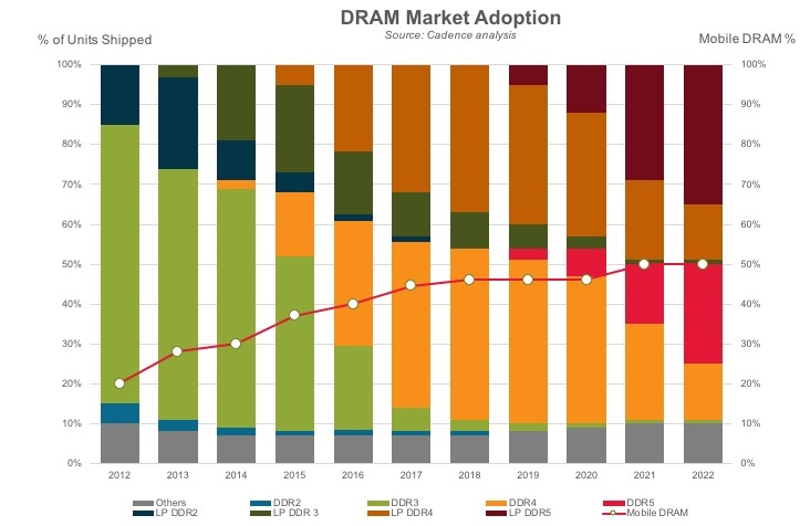
The first SoCs (system on chip) incorporating the DDR5-4400 IP are expected to be released as early as 2019, with DDR5 projected to overtake DDR4 by 2022.
If you’re as excited to develop SoC memory subsystems for the next generation of DDR5 RAM as we are, here’s how you can prepare.
DDR Basics
If you’re already familiar with how DDR works, feel free to skip this section to learn more about using our verification IP. For the beginners, this breakdown is for you.
A 2018 MacBook Pro sports a 2400MHz DDR4. Our DDR5-4400 IMC clocks in at a double data rate (DDR) of 4400MHz. Notice the pattern? The naming system DDRx-yyyy tells you the generation “x” and the DDR clock rate “yyyy.”
Why is it called a double data rate? Because DDR memory can send and receive signals twice per clock cycle, or double the rate of the original SDRAM (Synchronous Dynamic Random Access Memory). So the real maximum clock rate of a DDR4-2400 is 1200 MHz and DDR5-4400 is 2200 MHz. It just does twice the transfers or 4400 MT/s at this clock speed.
Now that you know what signal speeds you’ll be dealing with, you’ll understand that designing for DDR5 inherently pushes the limits of high-speed serial interface testing methodologies. When DDR4 first entered the scene at 1,600 MT/s, it had a similar effect, so a good resource for anyone just entering the game is to see how people handled the DDR4 IP.
Another way to prepare for DDR5 is through solid high-speed PCB design. Here’s course that can help you get up to speed in 3 days.
What is a Verification IP or VIP?
When you really think about it, the performance of digital electronics really boils down to how well they’re able to interface with embedded and external sources of memory. The code that tells a device what to do has to be stored somewhere, and a device can only function if its able to pull those hard coded instructions from memory. This is why memory interface verification is so critical to the SoC development process.
A verification interface protocol or VIP let’s you do just that, verify your SoC’s ability to interface with a given memory model. There are VIP blocks for FLASH, USB, PCIe, MIPI, CCIX, and of course DDR SDRAM. An SoC developer will typically follow the Universal Verification Methodology (UVM) to verify that the different parts of their system can interface with the new standard.
At this early stage in the game, you’ll most certainly see design IP developers trying to be the first to implement a new specification or companies looking to be among the first to release products incorporating DDR5 RAM.
Eager to learn more about VIPs? Cadence is a leading manufacturer of VIPs, and offers training services in their customer support site provided you have an account.
Cadence VIP: DDR5 Memory Model
The Cadence VIP: DDR5 Memory Model supports the JEDEC® Memory Device DDR5 SDRAM standard that is still under development. Key features include:
-
Data Width: x4 and x8
-
Memory Density: 8Gb, 16Gb, 24Gb, and 32Gb
-
DDR Speed: 3200, 3600, 4000, and 4400
-
Bank Groups: x8 and x4
From general DDR functionality and timing checks such as initialization, bus timing, and read/write to single-cycle and two-cycle command decoding, it provides everything you might expect from a DDR SDRAM IP.
Conclusion
Whether you’re an in-house team working on a new design aimed at being the first to implement the DDR5 or simply an early adopter and avid SoC developer looking to push the envelope of electronics design, Cadence’s DDR5-4400 VIP can help prepare you for the next generation of DDR5 SDRAM.