Taking High Speed PCB Layout to the Next Level

Right now, printed circuit board layout is as challenging to accomplish as it has ever been. At the same time, it is also easier right now than it will ever be again. Progress marches on and rarely looks back. Has your PCB layout gone beyond the known and into the unknown? Has an entirely new specification come along and suddenly the data rate went from megabytes to gigabytes? Practices that once held up to scrutiny now fail to meet the design mask? These questions lead us to ponder how we can keep up with the increasing edge rates while living within the power requirements and emissions standards that tighten around our designs.
The word from the boardroom is that high speed digital design begins to resemble RF work somewhere around the 1 GB/s. Anything that happens a thousand million times per second had better have a very clean start and end for each piece of information. The way the signals move down the line changes from using the entire trace to flowing mostly along the outer perimeter of the trace when seen in cross-section. Many factors surround this phenomenon; it is not a simple matter. This “skin effect” brings us to wanting wider traces for more skin in the game. Wider traces has us recalculating the dielectric thickness to maintain the correct impedance. There goes the stack-up plan.
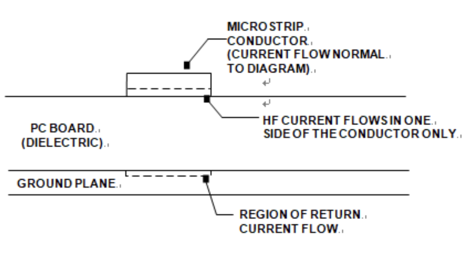
Image credit: Circuit Work
Make it Smaller
Signals propagate incredibly fast on a well designed transmission line. Even so, shorter is always better. Careful placement that is sympathetic to the critical path will make it easier to route with design margin to spare. Working around wider busses as with DDR is why I’m using the phrase “careful placement” rather than compressed placement. Overcrowded traces are a significant threat to signal integrity. Your own experience and simply diving into a fan-out study will help figure out the optimal layer-count and trace geometry for each unique situation. Factor in a little extra space to make higher speed connections behave themselves.
Once someone explains what they want from a layout, it is always tempting to sum it up for them like this. “So, you want all of the parts close together and all of the routing far apart?” That is basically it. Again, crafty placement followed by clever fan-out that alleviates the density hotspots will probably take a few iterations that don’t make it to prime time. Never be discouraged from improving the flow of a circuit. If you are lucky enough to see some simulations and how they are affected by small changes to the routing, you are gaining insights that will propel the next design forward.
Be Ready For the Next Voltage Swing
Lower voltage devices often have a lower noise floor. Don’t Fight the Power. Keep it handy in the form of shunt capacitors positioned near the power pin, and importantly, the other side of the cap wants to get cozy with a ground pin on the device if there are any in proximity. The whole path from the power pin through the cap and back to the device’s ground matters as it forms an inductive loop. The smaller that loop is, the better. The chip may be pinned out such that a specific pair of power and ground pins are a functional set. There may be many such pairings.
Paying attention to the application notes will help solve the power dilemma. When a company has an internal chip team, the architecture for PCB layout is often up to you to figure out. The ball-mapping session is the best time to find out about any vulnerable or particularly aggressive pins. If you can get into that review and influence the pin locations, it’s a golden opportunity to help the tightly focused team to consider the system architecture. It shouldn’t be a foreign concept, but for some folks, the word ends at the wafer. If all you can get is the XO pins moved out to the perimeter, it’s win. Do a good job on your reference designs, You never know who will be using them.
Prevent the Differential Pairs From Becoming Too Different.
Device makers and our Electrical Engineers are becoming more fond of loosely coupled differential pairs. There may be less mutual capacitance over longer runs than with tightly coupled diff-pairs. The air-gap between our diff-pairs is usually wider than the traces themselves which is the tipping point between tight and loose coupling.
With extreme rise and fall times, we have to become more aware of keeping the two members of each pair in tune with each other. The extra air-gap between the positive and negative traces gives more length advantage to the trace that is taking the inside of the curve. An S curve cancels out the differences, but a U-turn adds up. There are times when the best way to meander a pair is to run past its destination pin-pair and then come back. Avoid the temptation if at all possible. The inter-pair skew can add up to a millimeter which is an order of magnitude more deviation than the application notes generally allow. Balance the left and right bends as much as possible so you’re not exceeding the uncoupled length constraint with too many phase tuning bumps. It’s a balancing act with a vanishing margin for deviation.
Your guru (small g) mind trick, in this case, is to think about using dynamic phase control. What this entails is realigning the two traces every time there is a substantial turn. What we want is for the two waveforms to travel down each segment of the overall path in lockstep. A little bump in the trace that takes the shorter route is the crux of the technique. Just as we can’t float down the same river twice, the conditions present in an area change from instant to instant. We’re not just phase tuning so that the two signals reach the receiver pin-pair simultaneously, we’re keeping them synched from one end to the other.
Of course, we don’t want any vias on our high-speed traces. That said, if one member of a group gets one or two, the others should have sympathetic vias and route on the same layers. Outer layers slow the signals down relative to inner layers, and they offer less EMI and physical protection for the transmission lines. Keeping the propagation velocity the same by using the same topology is good. Traces that are virtually identical is better. Having a ground via near the high speed transition is good. Creating a coax in the Z-axis by surrounding the signal via(s) with three or more ground vias is the next level in EMI suppression. It takes more effort and time to do a job with margin to spare. Trying to retrofit quality into a failed design is even more effort. Investing in a solid design with a little extra breathing room pays much better dividends. Get you some!