Return Path Integrity in HDI Designs: How Microvias Reshape High-Speed Current Flow
Every high-speed signal has a return current, and the path that return current takes profoundly influences signal integrity, EMI, and system performance. In conventional through-hole PCB designs, return path management follows well-established patterns. HDI technology changes these patterns in ways that designers must understand to avoid signal integrity problems that seem to appear from nowhere.
How Return Currents Behave Through Microvia Transitions
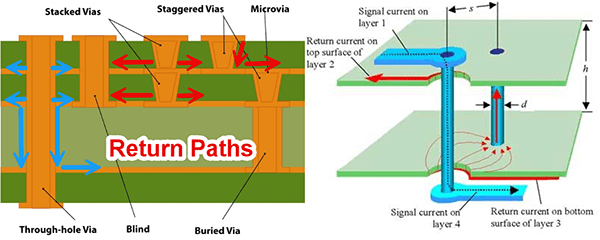
Figure 1: Ground return via. Vs. Image from " by Dr. Howard Johnson from " High-Speed Signal Propagation ", Fig. 5.33, p. 353. via Signal Consulting, Inc.
At all frequencies (including DC and AC), return current will follow the path of least impedance (resistance + reactance = resistance + inductance + capacitance). This typically translates to the following behavior (you’ll see this written often):
- At DC and low frequencies, return current follows the path of lowest resistance, typically the most direct route through available conductors.
- At high frequencies, inductance dominates and return current prefers the path of lowest inductance, which is directly beneath the signal trace on the nearest reference plane, regardless of whether that's the shortest resistive path.
When a signal transitions between layers via a through-hole via, its return current has a natural path: the same via (or an adjacent ground via) penetrates all planes, providing automatic return path continuity. The return current on the source layer's reference plane flows to the via barrel, travels through the via, and emerges on the destination layer's reference plane, near the signal path.
Microvias connect only adjacent layer pairs. A signal transitioning from layer 1 to layer 4 cannot use a single microvia, it must traverse multiple vias (1→2, 2→3, 3→4) either stacked or staggered. At each transition, the return current must also change reference planes. Without explicit provision for these transitions, return current is forced to find alternative paths.
These alternative paths are never optimal. Return current may flow laterally across a plane to reach a distant via that connects to the needed reference, creating a large current loop that radiates electromagnetic energy and adds inductance to the signal path. Or return current may couple capacitively between planes, introducing frequency-dependent impedance variations.

Uncover how return path design impacts signal integrity and how stitching vias can prevent performance issues.
Stitching Strategies for Signal Integrity
Uncover how return path design impacts signal integrity and how stitching vias can prevent performance issues.
Effective return path management in HDI requires deliberate stitching, with ground vias placed specifically to provide return current paths at every signal layer transition.
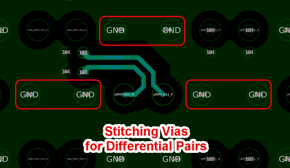
Co-located stitching: Place a ground microvia immediately adjacent to each signal microvia, using the same via type and connecting the same layer pairs. The distance between signal and ground vias determines loop inductance. Closer is always better. For critical signals, target stitching via placement within 20 mils of the signal via.
Via pair patterns: For differential pairs , the stitching strategy should maintain symmetry. A common approach places one ground stitching via between the P and N signal vias, with additional ground vias flanking the pair. This creates a GSG (ground-signal-ground) or GSSG pattern through the via transition.
Multi-level stitching: When signals traverse multiple microvia levels, stitching must follow. If a signal uses stacked microvias from layer 1 through layer 4, the adjacent ground stitching must also stack through the same layers. Stitching that stops partway leaves return current stranded.
Plane-to-plane stitching arrays: Beyond individual signal stitching, distributed via arrays that connect reference planes throughout the board reduce overall plane-pair impedance and provide multiple paths for return current redistribution. In HDI designs, these arrays must use via types appropriate to each plane pair, such as microvias where planes are on adjacent layers, buried vias or through-vias where planes are separated by multiple layers.
Avoiding Return Path Traps Under Dense BGAs
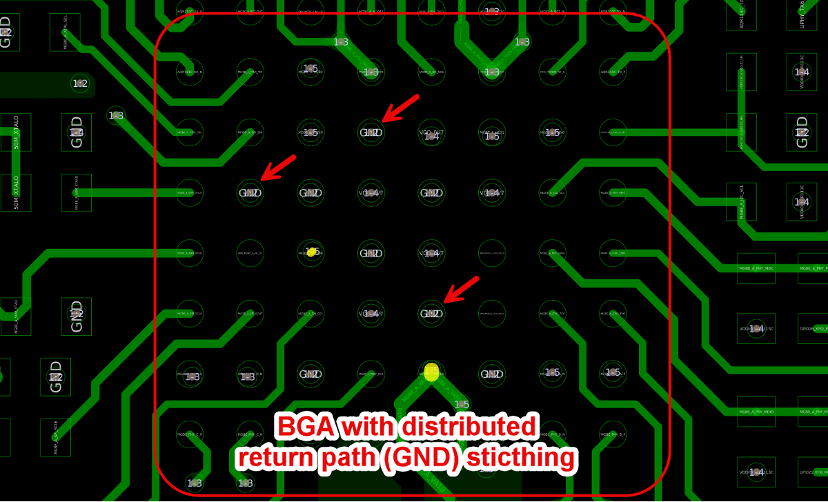
Figure 3: BGA footprint showing distributed ground stitching (good)
The region beneath a fine-pitch BGA presents some highly-specific return path challenges. Signal vias are densely packed; every available location seems consumed by signal escape routing. Ground stitching competes for the same limited space.
Common return path failures in BGA regions include:
- Stitching only at periphery: Ground vias placed only around the BGA edge leave signals in the BGA center with long paths to return current connection. Return currents from center signals must travel laterally to the edge, creating loops that radiate and add inductance.
- Insufficient ground pins: BGA pinouts that skimp on ground pins force multiple signals to share return paths through distant ground vias. Review the BGA pinout early; if ground pin distribution is inadequate, work with the component vendor or add PCB ground vias where the BGA ground pattern permits.
- Reference plane discontinuities: Power plane splits or thermal relief patterns in ground planes beneath the BGA interrupt return current flow. Signals that cross these discontinuities experience impedance spikes and radiate at the crossing point.
The solution requires planning ground via locations as deliberately as signal via locations. For fine-pitch BGAs, this means treating ground pins as resources to be allocated across the BGA footprint, ensuring every signal cluster has nearby ground stitching.
Impacts on DDR5, PCIe Gen5/6, and USB4
Modern high-speed interfaces operate at data rates where return path deficiencies create measurable signal integrity degradation.
DDR5: Operating at 4800-8400 MT/s (and climbing), DDR5 data signals have edge rates under 100 picoseconds. Return path inductance from inadequate stitching manifests as ringing on data strobes and reduced timing margin. The byte-lane architecture of DDR5 makes symmetric return paths within each byte lane critical, as asymmetric stitching creates a skew between the DQ and DQS signals.
PCIe Gen5/6: At 32 GT/s (Gen5) and 64 GT/s (Gen6), PCIe lane signal integrity depends on maintaining differential impedance through every via transition. Return path discontinuities convert common-mode noise to differential-mode noise that closes the eye. The equalization built into modern PCIe receivers can compensate for some degradation, but inadequate return paths consume equalization headroom that would better serve channel loss compensation.
USB4: USB4's tunneling architecture multiplexes multiple protocols over a single physical layer operating up to 40 Gbps (USB4 Gen3). The protocol's reliance on precise timing for tunnel arbitration makes jitter from return path deficiencies particularly problematic. USB4 designs require disciplined return path management throughout the signal path, from connector through vias to controller BGA escape.
For all these interfaces, return path analysis should be part of the standard design review process. Simulation tools can extract the additional inductance from non-ideal return paths and model its impact on signal integrity metrics.