Why PDN Failures Rarely Come From 'Too Few Capacitors'
You have a voltage rail that fails to stay within tolerance under load. The first instinct is to add more decoupling capacitors. More capacitance should mean more charge available, which should mean less voltage noise. So you add ten more 0.1 uF caps near the IC. The problem does not improve. You add ten more. Still no improvement. What is going on?
The issue is almost never the amount of capacitance. The issue is the inductance of the path between the capacitor and the IC. That inductance is set by the physical layout: how long the traces are, how the vias connect to the planes, and how far the current must travel to complete the loop. Adding more capacitors without fixing the loop geometry adds more capacitance behind the same inductance bottleneck.
Trace the Full Current Loop
A decoupling capacitor works by providing a local reservoir of charge near the IC. When the IC switches and demands a burst of current, the capacitor supplies it. But the current must complete a full loop. It flows from the capacitor's positive terminal, through the trace and via to the IC power pin, through the IC, out the IC ground pin, through the ground via and trace back to the capacitor's negative terminal. Every conductor in that loop has inductance.
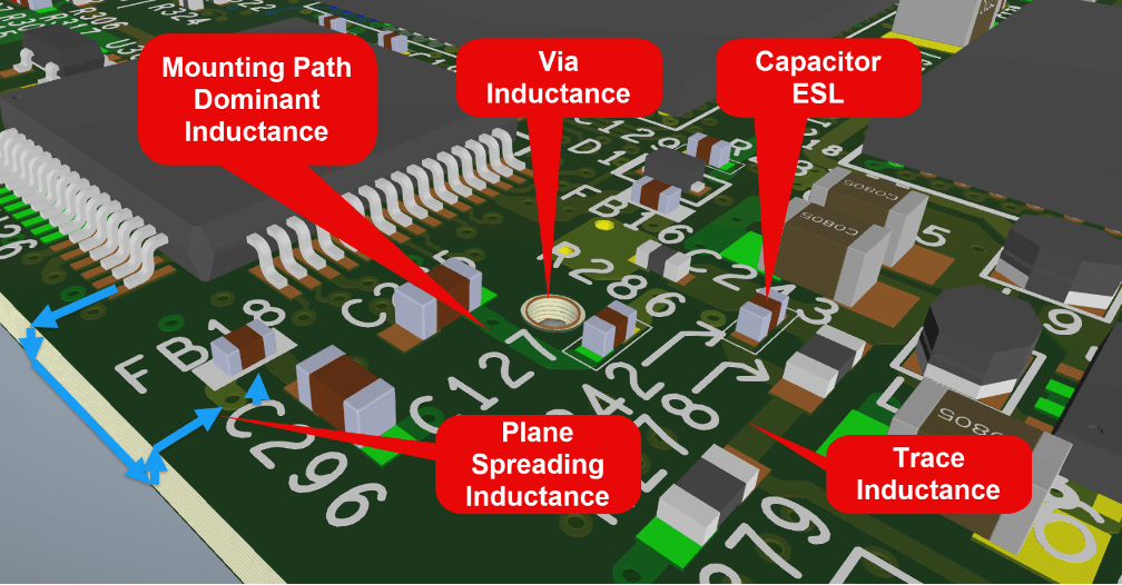
Figure 1: Diagram showing the full current loop from a decoupling capacitor to an IC and back. Annotate each inductance contributor: capacitor ESL, trace inductance, via inductance, plane spreading inductance. Show that the mounting path dominates.
The total loop inductance is the sum of several pieces. First, the equivalent series inductance (ESL) inside the capacitor itself. For a typical ceramic chip capacitor, ESL is around 1 nH. Second, the trace inductance from the capacitor pads to the vias that connect to the power and ground planes. Third, the via inductance, which depends on via diameter, via height, and the distance between the power and ground vias. Fourth, the spreading inductance in the planes between the via landing and the IC connection.
The Sierra Circuits High-Speed PCB Design Guide provides formulas for each of these. Via loop inductance for a pair of vias with diameter d, separation D, and height h is approximately: Lvp = 0.4 x h x [ln(2D/d) + 1/4] nH, where h is in millimeters. For an 8-mil diameter via with 40-mil center-to-center spacing and 60-mil height (1.5 mm), the via loop inductance alone is about 1.53 nH. That is already larger than the capacitor's own ESL.
This means the via and trace connections dominate the total loop inductance. The capacitor's internal ESL is typically the smallest contributor. Improving the capacitor does nothing if the mounting geometry is the bottleneck.
Why More Capacitors Stop Helping
A real capacitor behaves like a capacitor only below its self-resonant frequency. At that frequency, the capacitor's ESL and capacitance form a resonant circuit, and the impedance reaches its minimum value (equal to the ESR, the equivalent series resistance). Above the self-resonant frequency, the capacitor's impedance increases with frequency because the ESL dominates. It stops being a capacitor and starts acting like an inductor.
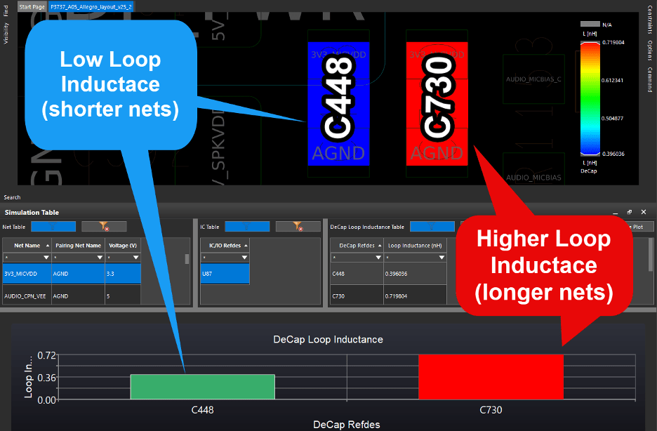
Figure 2: Power Inductance Workflow results from Sigrity X Aurora showing loop inductance values for two capacitors on the same net. One has low loop inductance (short mounting traces). The other has high loop inductance (longer traces). Annotate the difference.
For a typical 0.1 uF ceramic capacitor, the self-resonant frequency is in the range of 10 to 30 MHz. Above that frequency, the capacitor's impedance rises. Putting more 0.1 uF capacitors in parallel reduces the effective ESL and ESR (each divides by the number of caps), which extends the useful range somewhat. But the mounting inductance of each additional capacitor still adds to the total. If the trace-and-via loop inductance for each cap is 2 to 3 nH, paralleling ten capacitors still leaves you with an effective loop inductance of roughly 0.2 to 0.3 nH from the mounting alone, on top of the shared plane spreading inductance.
At frequencies above a few hundred megahertz, the mounting inductance of every capacitor in the array is the limiting factor. No amount of additional capacitance changes the mounting geometry.
What Fixes the Problem: Shorter Loops, Not More Caps
The Sigrity X Aurora Power Inductance Workflow measures the loop inductance from each decoupling capacitor to its associated IC. In the Sigrity X Aurora training course, two capacitors on the same board and the same net showed very different loop inductance values. The difference came from the physical mounting: one capacitor had short, direct traces to the power plane vias. The other had longer traces. The longer traces created a larger current loop area and a higher loop inductance.
The fix is layout-driven. Reduce the loop area. That means shorter traces from capacitor pads to vias. Vias placed as close to the capacitor pads as possible, ideally directly in the pad (via-in-pad). Power and ground planes on adjacent layers with minimal separation, which reduces the spreading inductance. And the capacitors themselves are placed as close to the IC power pins as the layout allows.
The Sierra Circuits guide puts it simply: to keep trace loop inductance low, keep the trace length short, keep the trace width wide, and keep the height between the component layer and the reference planes small. All three reduce the characteristic impedance and propagation delay of the loop, which directly reduces the inductance.
The Planes Themselves Are Capacitors
At frequencies above a few hundred megahertz, the capacitance between a power plane and an adjacent ground plane becomes a significant contributor to PDN performance. This plane-pair capacitance depends on three things: the area of the overlapping planes, the separation between them, and the dielectric constant of the material between them. Closer spacing and larger area both increase the capacitance.
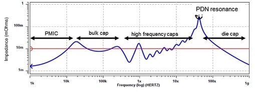
Figure 3: PDN impedance vs. frequency plot showing the target impedance line. VRMs (e.g. power management ICs - PMICs) are at low frequency, bulk caps at mid frequency, ceramic caps above that at high frequencies, die capacitors at even higher frequencies, then plane capacitance at high to very high frequency. (Source: Cadence Blog)
This plane capacitance is useful because it has almost zero mounting inductance. The current does not need to travel through traces and vias to reach a capacitor. It is distributed across the entire plane area. This makes plane-pair capacitance effective at higher frequencies where discrete capacitors have become inductive.
The stackup design, made in the Cross-Section Editor, directly controls this. Placing a power plane and ground plane on adjacent layers with thin dielectric spacing (3 to 4 mils) provides significant built-in decoupling with very low inductance.
PDN Design Is a Geometry Problem
Power delivery network (PDN) impedance is controlled by physical geometry. The loop area of the capacitor mounting path. The via diameter and spacing. The plane separation. The trace length and width. These are layout decisions. They determine whether your decoupling strategy works or whether you are adding capacitors behind an inductance wall that prevents them from doing their job.
Sigrity X Aurora measures these quantities directly from the routed layout. The IR Drop workflow shows where current density is highest. The Power Inductance Workflow shows which capacitors have high loop inductance and identifies poor mounting as the cause. The fix is always a layout change, not a bill of materials (BOM) change.