How Does Allegro X Support Button Plating?
Button plating, also referred to as pads only plating, is a selective copper plating process that limits copper buildup to plated through-hole barrels and their surrounding pads, rather than applying it across the entire board surface. If you have worked on a flexible circuit or other flex PCBs, you have likely encountered PCB button plating requirements as soon as a plated through-hole is introduced into the printed circuit board. The concept itself is straightforward. The challenge is making sure your PCB design communicates that intent clearly enough for the PCB manufacturer to build it correctly.
Most issues with the button plating process are not caused by fabrication limitations. They occur when the fabrication data does not clearly define how copper plating should be applied. When that happens, the PCB manufacturer typically defaults to panel processing across the outer layers, which can significantly change both mechanical behavior and electrical performance.
What’s Driving the Need for Selective Plating
To understand why selective processing is necessary, it helps to look at how a typical printed circuit board is fabricated.
In standard rigid PCBs, the process includes panel processing, where copper deposits are applied uniformly across the entire flat surface of the outer layers. This increases copper thicknesses on all exposed features, including traces, pads, and vias.
That works well for rigid PCBs, but it introduces problems in a flexible circuit.
Flex PCBs use roll annealed RA copper as their base copper because of its grain structure. The grains are aligned to support repeated bending without cracking. When additional copper is built up across that surface, it creates a stiffer composite structure. This added stiffness directly reduces flexibility in areas that are designed to bend.
There is also a geometric impact. During this step, copper deposits grow both vertically and along the sidewalls of features. This produces a trapezoidal profile, increasing both trace width and thickness. As a result, spacing between adjacent features decreases, and stiffness increases across the outer layers of the printed circuit board.
The button plating process, also referred to as pads only plating, solves these issues by confining copper buildup to the plated through-hole regions and their pads. Instead of coating the entire flat surface, the process is configured to reinforce only the areas that need it.
This allows the rest of the circuitry to remain at its original base copper thickness, preserving flexibility and maintaining the geometry defined during PCB design.
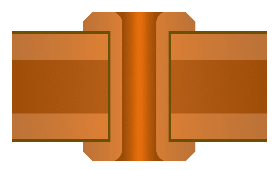
Figure: Cross-section view of a button-plated via: additional copper deposits at the barrel and pad regions only, with surrounding layers remaining at base copper thickness.
Understanding the Fabrication Sequence
From a fabrication standpoint, the sequence is straightforward, but it depends heavily on how clearly the PCB design communicates intent to the PCB manufacturer.
After drilling, a thin conductive seed layer is deposited across the entire printed circuit board, including the walls of each plated through-hole. This layer enables subsequent copper buildup.
A resist layer is then applied and patterned so that only the plated through-hole barrels and pad regions remain exposed. This defines where additional copper deposits will form.
Electrochemical deposition is then used to build copper in these exposed regions, increasing copper thicknesses locally. Because this step is selective, the surrounding flat surface retains its original base copper thickness and mechanical properties.
Once the target thickness is reached, the resist is removed and the remaining base copper is etched to form the final circuit.
The result is a printed circuit board where reinforced regions appear slightly raised relative to the surrounding copper. This localized structure defines PCB button plating.
If this intent is not clearly defined, the PCB manufacturer will typically apply full panel copper plating, increasing copper thicknesses across the entire board. That can reduce flexibility and introduce unintended electrical variation.

Figure: Cross-section of a button-plated PTH in a two-layer flex stack-up. Electrodeposited copper is confined to the via barrel and pad plating rings. Both RA copper layers remain at base copper thickness, preserving the grain structure and bend compliance of the surrounding flex circuit.
Defining Button Plating in Allegro X PCB Layout
In Allegro X PCB Layout, selective copper buildup techniques like PCB button plating are defined in the Cross Section Editor using Mask Layers.
These layers indicate where fabrication steps such as copper plating are applied within the printed circuit board stack-up. Padstack features placed on these layers define the reinforced regions at each plated through-hole, and that information is passed directly to the PCB manufacturer through fabrication outputs.
One point that often causes confusion is the term “Mask Layer.”
Many designers associate it with solder mask or other non-conductive materials. In this context, the definition is broader. A Mask Layer defines where a process applies, not what material it represents.
That distinction is critical. The layer is not describing a physical coating. It is defining where copper buildup occurs on the outer layers, effectively controlling where copper deposits are formed within the printed circuit board.
If this is misunderstood, the intended button plating process may not be implemented correctly, and the PCB manufacturer may default to full panel processing.
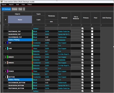
Figure: Allegro X Cross Section Editor showing a six-layer rigid-flex stack-up with Button Plating Mask Layers positioned at the top and bottom surfaces. This layer definition controls where copper deposits are applied during fabrication, limiting buildup to the via barrel and pad annular rings rather than the full outer layer panel.
Setting Up Your Plated Vias
In real-world PCB design, it is common to have a mix of standard vias and selectively reinforced vias of the same nominal size.
A practical approach is to define dedicated Mask Layers for each surface that requires this process, such as Button_Plating_Top and Button_Plating_Bottom.
Next, create a separate via definition. For example, if a standard plated through-hole uses a 6 mil drill, define the selectively reinforced version as 6.01 mil. This small offset allows the vias to be distinguished in the database while remaining functionally equivalent for the PCB manufacturer.
This approach provides several benefits. It makes vias easier to identify during layout, ensures that artwork includes only the intended features, and allows separate drill outputs if needed.
The result is a fabrication package that clearly communicates intent across the Cross Section, artwork, and drill data.
Key Design Considerations
Several design factors directly impact reliability when using selective copper buildup in a flexible circuit.
Bend radius is one of the most important. Even with localized copper reinforcement, tight bends concentrate stress at the plated through-hole, which can lead to cracking over time.
Material selection is also critical. Using roll annealed RA copper with appropriate copper thicknesses ensures the printed circuit board maintains flexibility while providing sufficient strength.
Trace routing should follow the grain direction of the base copper whenever possible. Routing perpendicular to the bend axis increases fatigue risk.
Finally, controlling copper deposits inside the plated through-hole is essential. Too little copper reduces reliability, while excessive buildup can affect tolerances. The controlled nature of pads only plating helps maintain this balance.
Why It Matters Beyond Flex
While most often associated with flex PCBs, button plating is also valuable in other printed circuit board applications.
One of the key benefits is improved impedance control. In high-speed PCB design, trace geometry directly affects signal integrity. Uniform copper buildup across traces after imaging changes both width and thickness, which can shift impedance.
With pads only plating, trace dimensions remain stable because additional copper deposits are not formed on the traces. This helps maintain predictable impedance across the printed circuit board.
There is also a layout density advantage. Since copper deposits are confined to vias and pads, spacing between traces on the outer layers is controlled entirely by the etching process. This enables tighter routing and better utilization of space.
In addition, designs that require strong plated through-hole structures without increasing copper across the entire printed circuit board benefit from this selective approach.
Practical Takeaway
If your PCB design includes a flexible circuit with plated through-hole structures, confirm early whether PCB button plating is required.
Once confirmed, the priority is clearly defining the button plating process within the printed circuit board design data. Using Mask Layers, consistent via definitions, and aligned outputs ensures the PCB manufacturer applies copper plating correctly.
Most issues do not show up during layout. They appear during fabrication review, when assumptions are made about how copper deposits should be applied. Clear definition upfront helps avoid those issues and ensures the final printed circuit board meets both mechanical and electrical requirements, including impedance control.
If you’re looking to learn more about the Allegro X PCB platform, talk to our team of experts or subscribe to our YouTube channel.