PCB Routing Topology Matters More Than Speed
You can have two signals on the same board, running at the same data rate, through the same stackup, driven by the same IC, and get completely different signal quality results. One passes. One fails. The data rate did not change. The material did not change. The driver did not change. But the routing topology did.

Figure 1: Various signal traces in a high-speed complex HDI PCB
Topology , in this context, means the physical routing architecture of the signal path: which layers the trace uses, how many times it transitions through vias, which reference planes it runs against, and how those planes connect to each other. These physical details determine the electrical behavior of the channel. And they matter more than the data rate in predicting whether a signal will work or fail.
What Topology Means in PCB Layout
On a schematic, a net is a logical connection between two pins. A differential pair is two nets that travel together. The schematic tells you that pin A connects to pin B. It says nothing about the physical path.
In the layout, that same net has a physical topology. The trace starts on a specific layer, runs a specific length, transitions through vias to other layers, and references specific planes along the way. Every one of those details affects the electrical behavior of the signal. The topology includes the trace segments, the vias, the reference planes, and any discrete components connected along the path.
A topology is defined as a logical representation of the nets in your design. It includes the drivers and receivers, the passive interconnects that make up the transmission lines and vias, and any discrete components used for termination. This is the electrical model of your physical routing.
Two Differential Pairs, Same Board, Different Outcomes
The high-speed HDI PCB design below demonstrates this clearly. The design contains two USB data differential pairs: P0_USB and P1_USB. Both are on the same board. Both use the same stackup. Both connect to the same type of interface. The only difference is how they are routed.
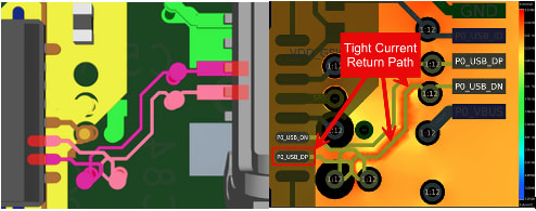
Figure 2: P0_USB diffpair P0_USB_N changes two layers and maintains a tight return current path. (Left: 3D routing view in Allegro X. Right: Return Path Vision view from Sigrity X Aurora)
P0_USB, the first differential pair, changes two layers. Its routing stays close to the top of the board. The return current on the L4_GND reference plane follows the signal path tightly, concentrated directly underneath the trace.


Figure 3: P1_USB changes nine layers and four reference planes. The return path quality degrades with each transition. Top: 3D routing view showing the P1_USB differential pair. Middle, Bottom: Nine layer transitions across four reference planes. Return current is spread across multiple planes (L9 tighter return path, L2 looser return path).
P1_USB, the second differential pair, changes nine layers across four reference planes before returning to the top layer. Every time the signal transitions to a new layer, the return current must also transition to a new reference plane. Each of those transitions adds inductance to the return path and spreads the current over a wider area.
After running the Return Path workflow in Allegro X PCB Layout using the Sigrity X Aurora workflow , both pairs were assigned a Return Path Quality Factor (RPQF). RPQF is the ratio of the actual loop inductance to the ideal loop inductance. An RPQF of 1.0 represents the ideal case. As the return path becomes less ideal, the RPQF increases.
Even after all standard DRC violations were resolved on the board, the RPQF difference between P0_USB and P1_USB remained significant. In this PCB, as with any board, the quality factor difference between the two differential pairs persisted because of the routing used for each circuit. The P0_USB circuit changed two layers. The P1_USB circuit changed nine layers across four reference planes. The routing topology created the quality difference.
Why the Return Path Drives the Outcome
At all frequencies, the return current appears where the fields have found the path of lowest impedance, which means if you provide a path to ‘ground’ in a PCB stackup , it flows on the reference plane directly under the signal trace.
This is usually the tightest possible current loop (unless you have a trace closer to your signal than the GND plane is). Any disruption to that path forces the current to detour, increasing the loop area and adding inductance.

Figure 4: PCB stackup in Allegro X PCB Layout Cross-section editor
Because the electromagnetic field finds the nearest low impedance conductor, the return current for high-speed signals tries to follow the original signal path (e.g. Layer 1 signal has a ‘copy’ of it along Layer 2 ‘ground’). An incorrect signal return path (one that is not solid, adjacent to the signal layer and connects to GND) is one of the most common sources of noise coupling and EMI issues. High-speed signals should not be routed over a split plane because the electromagnetic field will find its own lowest impedance ‘return path’ and in most cases, we’re not going to like where it finds it. The field will meander wherever it needs to and thus not directly follow the original signal in the signal trace for its ‘return current’. That meandering is the source of common EMI issues .
Not only that, when a signal changes layers, the electromagnetic field is traversing that dielectric material between copper layers and is also changing reference planes. That layer transition requires a low-impedance path between the two PCB layers (signal, GND). A stitching via placed close to the signal via provides that shorter path for the electromagnetic field to find a nearby conductor material that gets the field to a low-impedance path as soon as possible, which is usually GND. Without it, the return current must find an alternate route to that same GND, thus spreading the field everywhere it so pleases, thus forming return path currents in multiple areas and increasing the loop inductance. So here is a strong recommendation for all PCB designs: stitching vias should be placed close to the signal via whenever a layer change occurs, and it is ideal to place the ground via right between the signal vias when possible.

Figure 5: Constraint Manager view showing the stitching via constraints applied to both USB differential pairs. Show the 'Missing Stitch Via' violations flagged on P1_USB. Standard DRC does not catch return path issues. The Return Path constraint and workflow does.
For differential pairs, the situation has another layer. In an ideal differential pair, the return current flows on the partner trace, and no current flows on the reference plane at all. But real differential pairs are never perfectly balanced. Unmatched impedance and length between the P and N legs cause common-mode current to flow on the ground plane. Even though the return path of a positive (DP) net would ideally be the negative (DN) net, unmatched impedance and length cause current to flow through the ground plane. That ground plane return path needs to be low impedance, which means continuous planes, length matched trace pairs, and stitching vias at every layer transition.
What This Means for Your Routing Decisions
Here are four practical rules for any PCB layout.
First, minimize layer transitions. Every layer change adds a via, adds a reference plane transition, and adds return path inductance. The P0_USB circuit with two layer changes had better return path quality than the P1_USB circuit with nine layer changes. Fewer transitions means cleaner return paths.
Second, place stitching vias at every signal layer transition. The Sierra Circuits guide and the Allegro X HDI design workflow both require this for high-speed signals. A stitching via connects the old reference plane to the new one, giving the return current a low-inductance path to follow the signal.
Third, avoid routing over split planes or plane voids. If the reference plane has a gap directly under the signal trace, the return current will now show up underneath or beside the signal directly. The electromagnetic field created from that signal must detour around the gap until it finds its referenced return path, thus increasing the loop area. Signals should not be routed over a split plane. Route around it.
Fourth, check the return path during layout, not after. The Return Path workflow in Sigrity X Aurora calculates the RPQF for every net and shows a current density visualization on each reference plane in IR drop analysis . You can identify return path problems while you can still change the routing, before the design goes to fabrication.
Topology Is the Variable You Control
Data rate is set by the interface specification. The stackup material is chosen early and usually stays fixed. The ICs are selected by the system architect. What you control as a layout engineer is the routing topology: which layers, which vias, which reference planes, how many transitions. Those decisions determine the return path quality, and the return path quality drives signal integrity outcomes.
Same board. Same speed. Different routing. Different results. Topology is the variable that matters.