Taming Electromagnetic Interference on Your PCB - What’s All This Noise?
You can’t always hear it, feel it or see it but every active electronic device is radiating some kind of energy as it operates. For the most part, that’s the point. We want to hear the music, we want to feel the air conditioning or see the light. Those are the good things.
Meanwhile there are side effects to good things that we don’t want. Static on the radio, compressor noise from the AC or that annoying 60 Hz hum out of the light fixture bleeding over to my new bass amp. It’s these things that we try our best to design out of the products we build.
We can try to adjust the tuner on the radio and we can install the central air conditioning unit away from the windows. I ordered a noise suppressor and plugged it into a different socket where there’s no dimmer switches or high current motors plugged in. Then the amplifier and the pedal board power cords get routed into the special apparatus and I no longer get a wave of white noise when this MacBook Pro is searching for a WiFi signal.
Even if the emissions cannot be perceived with our five senses, they can be detrimental to the performance of the circuit or they can spill out onto other nearby electronics. We use metal for the device housings for multiple reasons. Beyond the heat shedding property, we also want to keep our noise inside the box while preventing other noise from getting in. Those are the two central tenets of coexistence.

Image Credit: Author - My Blackboard with a new surge protector that also filters EMI and RFI.
If you want to chain a bunch of gain-stages together, it helps to start with clean power and a common ground path. The fix for noise issues is almost always additive. The new schematic you get just before the prototype goes for FCC certification usually has a new ferrite bead, maybe a diode here and there and some re-tuned bypass capacitor values.
Generally speaking there are a few factors that cause signal degradation. One of the main factors is long traces. The farther a signal has to travel the more likely it is to end up near a bad neighbor. In this case, bad can mean noisey or could mean susceptible to picking up noise. I’m tempted to open up that big, white, plastic wall-wart for this laptop to see if it has any shielding.
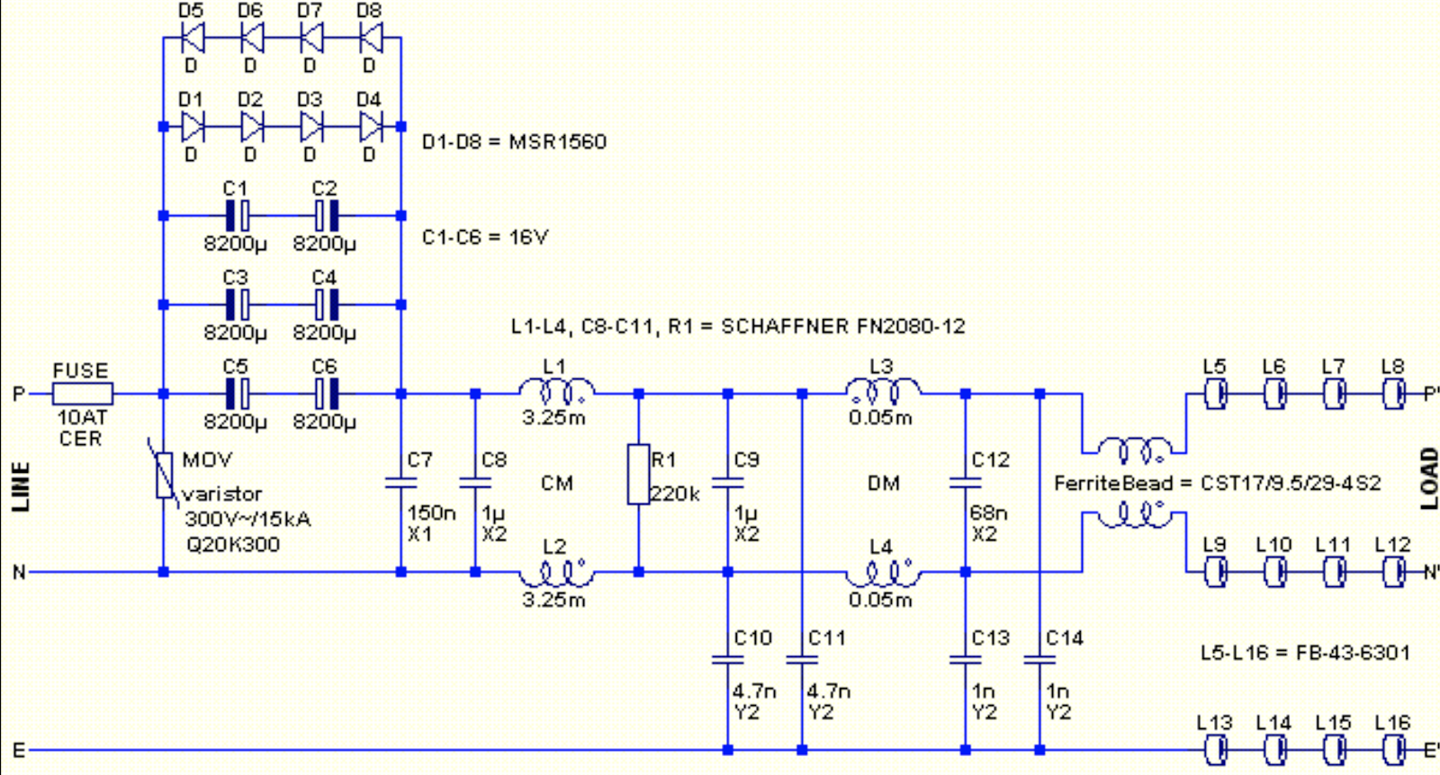
Image Credit: Audio Karma - These components are the typical building blocks of a noise suppressor circuit.
Getting the dirt out of the wall juice is the first line of defence. At the PCB level, the second line of defence is to shield the most vulnerable victim traces from exposure to the outside world. EMI shielding is carried out around the noise makers as well as the sensitive signals. One of the best ways to reduce coupling between those two types of elements is simply adding space.
Placement and orientation of components and printed antennas goes a long way towards mitigating noise issues. However, the luxury of a generous PCB is a rarity. No matter the amount of electronics, printed circuit boards cost money so less is more. Doing more with less is our existential challenge. A lot of designs will have an external oscillator so let’s take a look at that case.

Image Credit: Author - A crystal and it’s passive parts.
The crystal is placed close to the IC but it appears that we could achieve shorter traces by rotating the circuit by 90 degrees clockwise. Note the route keep-out that creates a moat that separates the outer layer ground plane from the pins of the crystal. Putting a ground via on the edge of the shape would defeat the purpose. Ideally, there would be one or more XO return pins for a direct ground path back to the SOC.
A mechanical outline for a PCB normally comes from a mechanical engineer with little to no electrical training. They might give us one part of the board where tall components are allowed. Wouldn’t you know it, the tall components include the crystal. All that thing does is sit there making noise so something has to be done with the long link back to the mothership.
Internal routing will be more effective than running an aggressor on the outer layers. That notion is predicated on the fact that there will be an unbroken ground plane both above and below the trace. Taking it a step further, a dedicated shape on the signal layer that encloses the trace is a good policy.
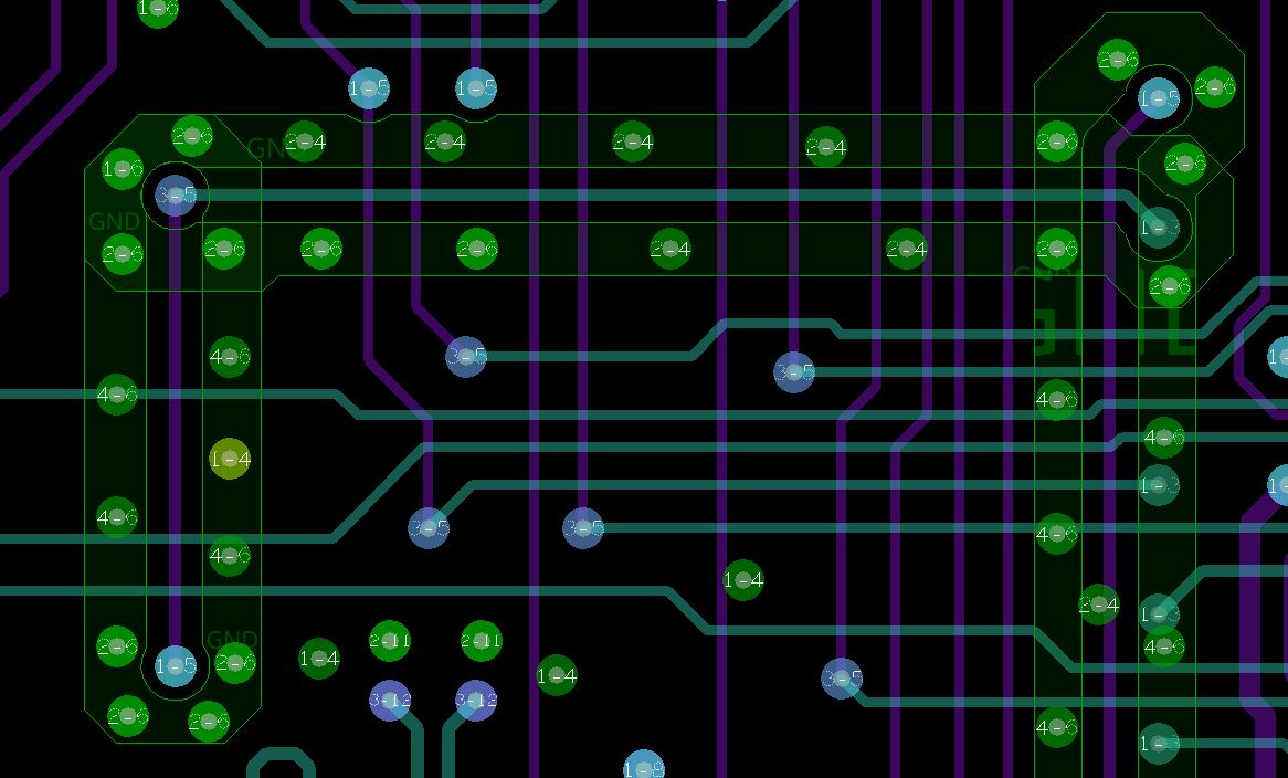
Image Credit: Author - Guard bands around noisy traces. The surrounding low-speed signals benefit from the isolation.
In the above figure, the ground net is highlighted in green. The cyan and magenta represent layers 3 and 5. The via labels indicate the span of the micro-vias. We want to tie the relevant ground planes together but not necessarily any other ground layers. If we were to flood ground on the routing layers, the full plane would not engulf these guard-bands. You might have noticed several signal vias without an adjacent ground via. The signals on both layers will see the ground plane on layer 4 so the ground via would be a feel-good measure.
Note that I used a 2-4 microvia stack for layer-three and a 4-6 microvia stack to shield the layer-five routes. Lastly, going beyond a single return via for the transition from layer three to layer five, there is a cluster of 2-6 vias around the 3-5 signal vias. The idea is to form a coaxial faraday cage in the z-axis. In cases where there isn’t this amount of space, do the best you can to isolate the noisy party.
We hear a lot about length-matching, phase tuning and taking care of the impedance of our high-speed connections. We know that vias are a discontinuity that we should avoid if possible. Routing over a split or void in the reference plane is a no-no. All of these impedance and timing rules are also necessary in order to keep the EMI to a minimum.
We’re also drilled with the fact that we want to keep our inductive loops small when we place and route bypass caps. We’re told to use multiple vias for power and ground planes. Alternating power and ground planes will transform the PCB into a bunch of free capacitors. These signal integrity and power integrity rules are there for the circuit performance reasons listed above but also to quell the emission of spurious radiation. Solid design practices help us bust the EMI and RFI problems.
Reducing crosstalk actually reduces power consumption. Making noise takes energy so suppressing the noise saves power. I mentioned up top that noise suppression is normally an additive process. Each of those resistive, capacitive and inductive elements has its own parasitic effects. It’s like adding cream and sugar to make the coffee less bitter. At a certain point, we lose the flavor of the coffee so we need a stronger brew.

Image Credit: Author - I like mine strong and black!
An elegant layout that accounts for potential energy transfer will not require as much cream and sugar on top of the essential circuits. The ground net plays a huge role. It’s definitely the most interesting net on the board. Vias are the one thing that prevents the ground net from taking on a charge from the other nets.
Staking down the edges of the ground planes including the voids makes for a PCB that runs more quietly and provides a substantial path for thermal dissipation. Once you’ve digested all of the basic rules around EMI, you’ll see PCBs in a different way. We can immediately spot it when an artist tries to draw imaginary circuits for a logo or whatever.
The average person will see the circles and lines and not know the difference. A trained designer will spot the flaws in a heartbeat. That goes beyond the artistic rendering and down into the nuances of memory routing or even chaining a bunch of guitar effects together to create a sound that I hear inside my head. I’m looking beyond the wires and connectors to think inside the box. That’s how a PCB designer sees the world.