Calculating PCB Circuit Density to Estimate Layer-Count and Required Technology
When I get a new design, one of the first things I want to know isn’t really if the architect is out of their mind. It’s more like “How far out of their mind are they?” The question is pertinent when all of the components are spread out around the border of the PCB. It’s most apparent with little dongles and daughter cards with ambitious circuits. Cell phones and other mobile devices are always going to be very ambitious so that there is more room for the batteries.
The first metric that comes to mind for PCB circuit density is the number of pins per square inch - or pick your unit of measure. The pins are a stand-in for both component and routing density. You may find the calculated values in a summary drawing report.
Otherwise, run the auto-placement function and then run a query finding only the pins. Jot that number down for the numerator. Calculating or extracting the available placement area will give you the denominator. Dividing the top by the bottom gets you the “something to one” ratio of PCB density. The higher that “something” number is, the more interesting the layout becomes. The higher number is like getting a merit badge; you’re going to have to earn it.
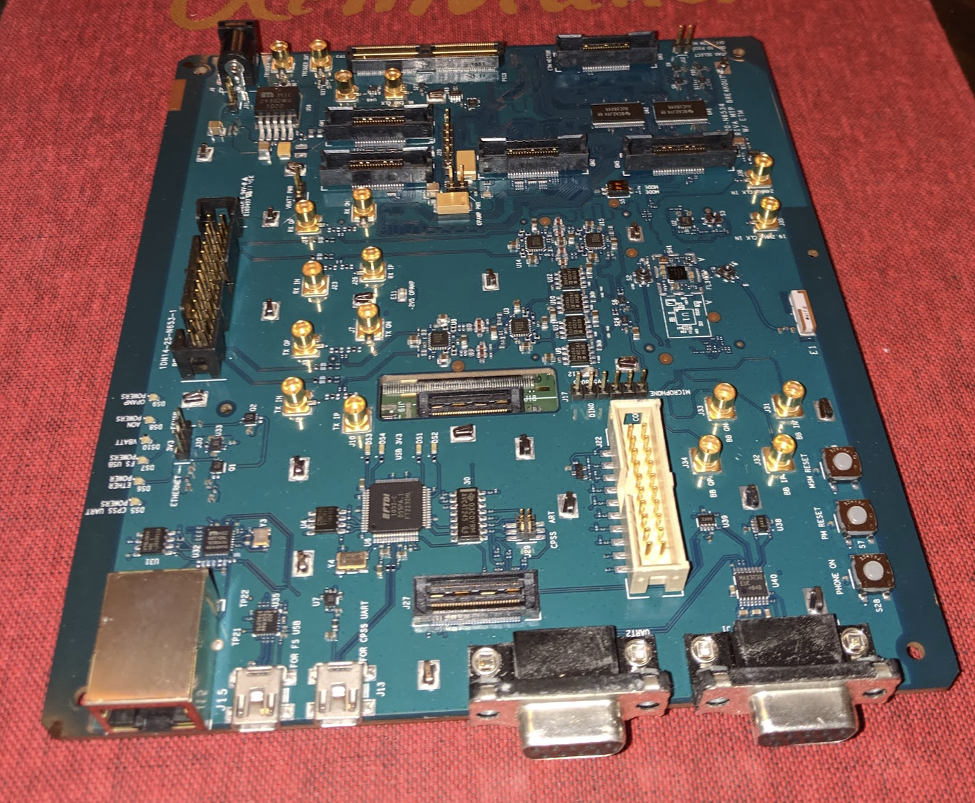
Image Credit: Author - Side rails for assembly are the first thing to go when density increases. They become part of the assembly sub-panel.
Comparing that ratio to some of your previous boards, particularly boards with similar functions, gives you a pretty good starting point for the number of layers and the type of technology will solve the puzzle. If the two density numbers are close, that’s the stack-up and geometry to use as a base line. If not, then consider the overall mix of components.
Using Both Sides of the PCB to Solve Density Limits
Of course, if the component density is well beyond the established norms, then you can double up the amount of available space by using both sides of the PCB. The product may have height limitations on the back side so it may only be available for the most low profile components. Using only the lightest components for the back side is better for assembly processing in any case. The earlier you can start the negotiation with the physical designer, the better. The historical data as a comparison is a good tool for making your case.
One of the main use cases for double sided PCBs is when there is a BGA or LGA involved. These packages often feature a host of power and ground pins situated near the location of the silicon. Those power pins on the die want to have bypass capacitors nearby. The smallest values are usually the most sensitive to proximity to the power and ground pins.
Mixed Signal Designs With a Reduced Form Factor
Mixed signal PCBs are another natural environment where the RF circuits go on one side and DSP resides on the other. There may be cases where you’d attach the relevant ground pins to one ground layer but not the one on the far side of the board. This is tricky in a through-hole PCB.
Say it’s a six-layer board with full ground on layers two and five along with flood over the outer layers. I would make one via with a square pad on layers 1 & 2 and another with a square pad on layer 5 & 6. Fanning out the top with square pads on layers 5 & 6 selected and the bottom with the other type leaves a visual cue for which via pads would need a void on the respective ground planes. You may be able to take advantage of other systematic tricks to solve this kind of dilemma on your board.
General Tips on Double Sided Placement
Putting parts on both sides of the board also presents a challenge to the assembly house. If at all possible, it is advisable to have all of the larger components on one side. Any component that is not robust enough to be soldered multiple times should join the larger parts. Typically, one side goes into the oven using a higher temperature solder then the other side goes in at a temperature profile that does not reflow the first side.
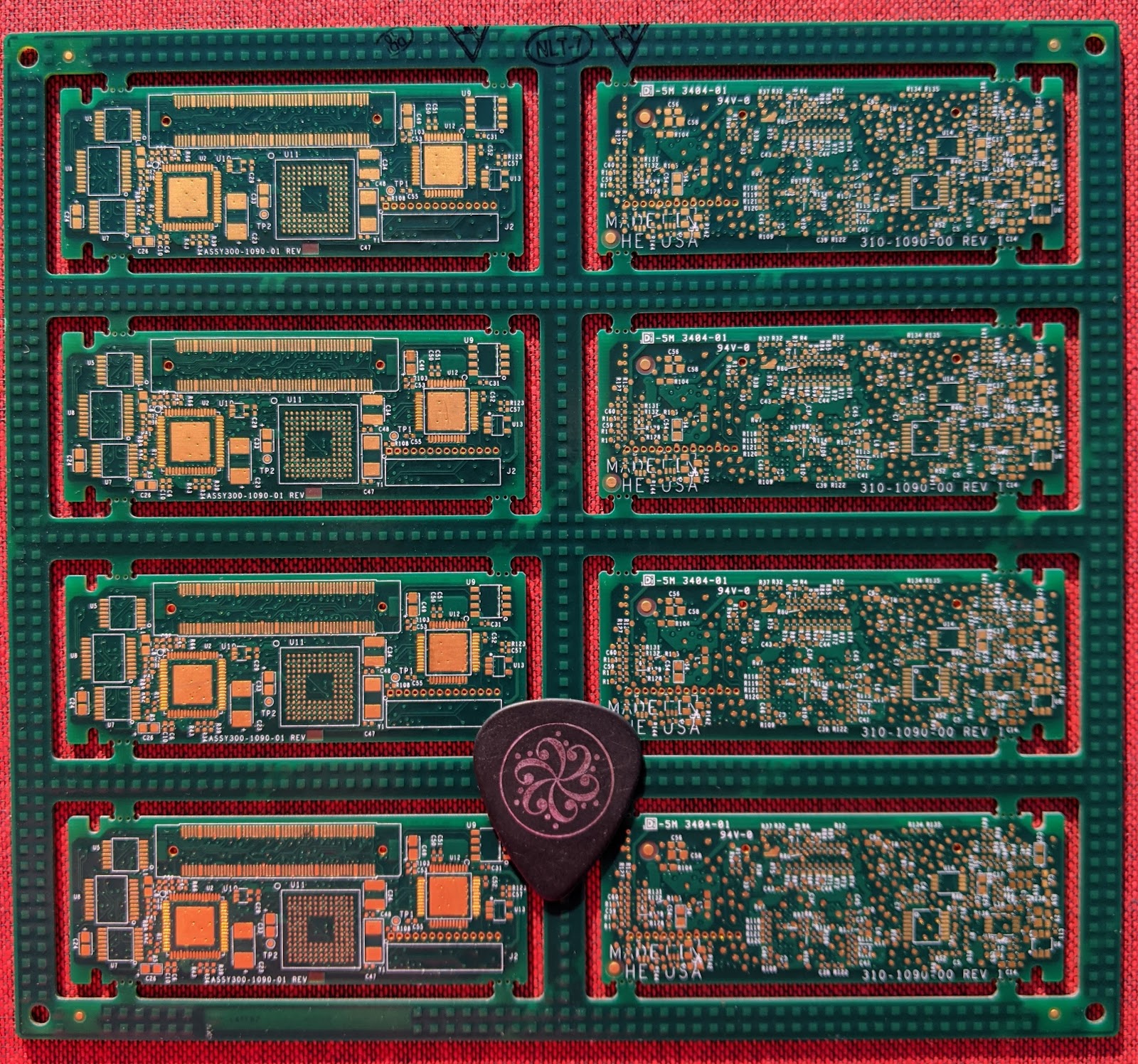
Image Credit: Author - Two sides of the same board with the small parts on the right side and the assembly rails on the break-off section. Note the thieving on the rails to even out metal distribution to mitigate warpage.
Circling back to the skill of estimating the technological requirements of a PCB without the benefit of hindsight gained from doing a previous iteration, I’ve compiled a short list of things to watch for.
Placement density factors include:
-
Component pitch of the processor and peripherals.
-
The size of the regulator circuits - and how many are used.
-
Shields and heat-pipes and other large non-electrical hardware
-
Significant component keep-out or head-room restrictions.
-
Sensors and antennas that require extra space and/or claim all of the layers below.
-
The general nature of the board; what does it do?
-
The IPC class; high reliability uses larger footprints.
-
Underfill, rework, or other assembly process novelties
If the components can be placed on the board without breaking the component spacing rules, then it can be routed. Reducing part size or count may be possible. Look for zero-ohm jumpers that might be replaced with an exacto knife and a jumper wire. Off-boarding the fiducials and tooling holes to the break-off areas of the assembly sub-panel may buy you additional room. Reducing the silkscreen to deprioritize reference designators and then part outlines may help but try to keep polarity marks as a last resort.
Consider the following items when evaluating the proposed routing technology.
Some things that will affect routing density:
-
Location and type of connectors
-
The overall flow of the signals; ideal vs. challenging placement
-
DDR or other wide busses that require significant serpentine and trace/trace spacing.
-
Hi Voltage or other abnormally large shape/air gap requirements
-
RF elements printed on the board
-
Holes or slots that neck down the routing channels
-
Class; the larger vias of Class 3 add up quickly.
-
Test access whether by boundary scan, in-circuit-test by bed-of-nails or flying probe.
-
And, of course, the type of board construction. HDI leads to thinner dielectrics which drive thinner controlled impedance and smaller geometries overall.
Keeping Everyone “On-Board” With the Risk/Reward Factors
Routing begins with fan-out. Fan out should have been accounted for during placement. The decision to go with via-in-pad-plated-over (VIPPO) would be made early in the design. This is a cost driver so the information regarding this decision needs to pass through the fab-shop to know the actual cost-hit. That information then needs to go to management so that they can make an informed decision on board size vs. production requirements.
Tightening up the placement in that way also involves the assembly house. Changing the library symbols from nominal to minimum size has an impact on producibility as well as rework and reliability. Sharing the placement with the assembly unit and their findings with the stakeholders is also advisable.
When we shrink down or add circuits to an existing form factor, there is risk to signal and power integrity. Thermal challenges and coexistence come into play. Schedules may be impacted by having to reiterate designs as you touch on new levels of component density. Whether it comes to more parts or parts with more closely spaced pins, there is a balance that must be maintained.
As you work harder on the design, the people downstream will also have to work harder to implement the design. The art of predicting where all of this goes right from the start is just one more skill that the designer should have as we move into the ever-shrinking world of the future. See you there!