Getting Started with Electrical Constraints in OrCAD X FAQ
Here are some comprehensive answers to all the questions asked in our recent webinar.
Constraint Management | General
Constraint Management
Yes, the same constraint manager seen in OrCAD X Presto is available in OrCAD X Capture and can be easily synchronized between your OrCAD X schematic and layout tools.
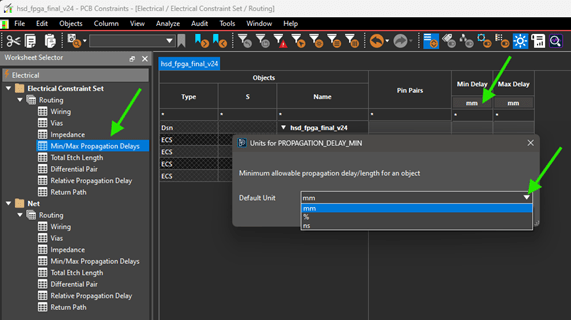
Net routing length constraints can be specified in terms of distance or delay time. Units available to select from are mm, %, and nano seconds (ns).
For a high-speed PCB, a recommended delta tolerance for trace impedance is typically around ± 10%; meaning the actual impedance of a trace can vary by up to 10% from the designed value, depending on the specific application and PCB manufacturing process.
To clarify, the target delay and impedance are independent of stackup data, meaning it will automatically update DRC checks based on the characteristics of the layer stack, but the targets remain constant.
The via count constraint is for vias that are connected to the net. If you have return path vias (like ground vias) that are used along with the signal via then you can use via structures and assign those as the via to use with the physical constraints.
Please contact technical support through this form for assistance.
Yes, you can set up constraints to verify that differential impedance is met or not within OrCAD X.
Currently all constraints are validated through the PCB DRC engine.
Creepage and clearance constraints are supported in our Allegro X toolset.
A Net Group is a collection of nets grouped together to facilitate performing an operation on the members, but they do not need to share constraints. A Net Class is only used to define constraints for the Net Class members. A Net Group can be a member of a Net Class.
Yes, assigning the constraint is possible with the Allegro X toolset. This video shows you how to set it up – keep in mind that the video is based on an earlier release of the product, but the concepts and workflows conveyed still apply to the current release of the product. So when you add vias while routing a diff pair they will be placed at the min-via to via spacing constraint that’s applied to the diff pair.
Please contact technical support through this form for assistance.
Yes, simply right click over the red box or net within the Constraint Manager worksheet and select cross probe from the menu. Make sure you are not in a command and also have the proper selection filters enabled; this ensures that you will jump directly to the corresponding location of the error in your layout.
Yes, you can. Please consult the following support article to see the steps required to enable Differential Impedance in Constraint Manager.
At this time there is no specific functionality where you can automatically calculate the trace width for a certain impedance depending on the type of transmission line. However, there is some basic functionality built into the Cross Section Editor where you can set the target impedance based on your stack up geometry, your dielectric constant it will calculate the width for you.
Impedance requirements should be defined before routing begins, so it is recommended to start as early as possible during your schematic capture and layout planning stages, that way you can easily identify if there are any errors that need to be addressed within your design. You can set your electrical constraints on the schematic side in OrCAD X Capture and transfer or synchronize them to the layout side, such as OrCAD X Presto as well.
General
Yes, it is. To transfer a design from OrCAD X Capture to AWR, you would typically export a netlist from OrCAD X Capture in a compatible format (like SPICE) and then import that netlist into AWR.
Yes, you can do that with our Allegro X product line using our enterprise data management system called Pulse. Pulse enables workflow based automated processes running on a server.
Yes, all of these constraints and more can be created and applied within Allegro X System Capture and can even be done in a team design setting.
Please contact technical support through this form for assistance.
Yes, we support 3 different types of surface roughness. You can include, or exclude, these variables in the calculations.
In this webinar, we were using the OrCAD X Professional tier to do the demonstration, some constraint options may not be available in the lower OrCAD X Standard tier.
In OrCAD X Presto, right-click on a symbol and choose Edit Footprint, this will allow you to change/update pin numbers.
Yes, we have extensive training on our PCB design products - OrCAD X and Allegro X. You can access all available training on the cadence.com site here.
You will have to export using IPC-2581 from Polar Instruments and import that file into OrCAD X Presto.
No, the line width and spacing for differential pairs will not be imported into the Constraint Manager.
Constraints are stored with the schematic. but you can also write the constraints out as a separate file if desired.
Yes, you can use the min/max prop delay for net based spacing and the design for assembly constraints for assembly based spacing.
The field solver will calculate the impedance based on what is in the design so the calculated values in Constraint Manager are specific to what conductors are in the design. The calculations in the cross section are influenced by specifying if a layer is a plane or signal layer.