High-Speed Backplane Design Considerations and Routing Guidelines
Key Takeaways
-
Choosing low-loss laminate material reduces insertion loss and maintains signal integrity at high data rates.
-
Proper routing techniques, including differential pair spacing and backdrilling, minimize crosstalk and reflections.
-
Effective power distribution and grounding improve EMI control and ensure stable high-current delivery.
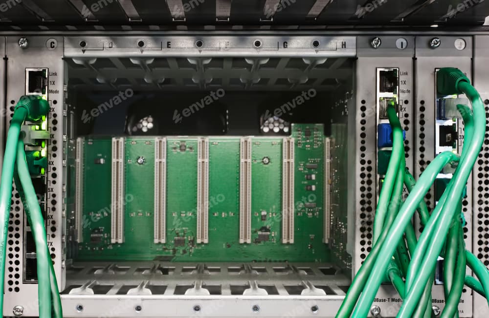
A network switch backplane with empty PCI slots and connected Ethernet cables.
A backplane is a circuit board that connects and allows communication between multiple circuit boards or modules. It provides pathways for data and power to flow between the boards, helping them work together as a system. Backplanes are commonly used in telecommunications, data centers, high-performance computing, and defense systems. This article provides insights on leveraging OrCAD X for high-speed backplane design, focusing on crucial design elements and routing guidelines.
Key Considerations for High-Speed Backplane Design
|
Consideration |
Key Design Guidelines |
|
Communication Standard Selection |
- Choose based on data rate, latency, and bandwidth needs. - Follow industry standards (e.g., PCIe, Ethernet, InfiniBand, VPX, RapidIO). |
|
PCB Stack-Up & Material Selection |
- Use low-loss laminates (e.g., Rogers, Megtron 6) to reduce insertion loss at 10 Gbps+ speeds. - Ensure symmetrical power/ground plane distribution. - Recommended dielectric constant (Dk) ≤ 4.4 to minimize signal degradation. |
|
Signal Integrity & Routing Strategy |
- Use differential pairs with 3W spacing, and ground pours between differential pairs - Minimize via transitions - Backdrilling vias eliminates stubs and enhances high-speed performance. - High-frequency traces should have stub lengths <1 inch to prevent reflections. |
|
Connector Selection & Pinout Design |
- Use high-speed, low-loss connectors (e.g., Samtec FireFly, Amphenol R-VPX, TE Connectivity MULTIGIG RT3). - Stagger signal pins; interleave ground pins to reduce crosstalk. - Row-by-row differential pair routing can reduce layers. |
|
Power Distribution & Grounding |
- Backplanes may supply up to 100A, requiring multiple power planes for stable delivery. - Separate high-speed signal layers from power layers to avoid interference. - Closely coupled ground planes to power planes reduce EMI and enhance return path integrity. |
|
Manufacturing & Testing |
- Perform impedance control testing to verify compliance. - Ensure backdrilled vias have <3 mil stub remaining. - Validate bit error rate (BER) and eye diagrams using high-speed oscilloscopes. - Use JTAG boundary scan & loopback testing. |
High-Speed Backplane Design Communication Standard
Designing a high-speed backplane requires careful planning to ensure signal integrity, power distribution, and manufacturability.
Define System Requirements and Communication Standard
To successfully design a high-speed backplane, it's essential to consider key system requirements and communication standards. Based on these factors, the following questions can guide the decision-making process:
-
Data Rate: What is the required speed per link?
-
Number of Connected Modules: How many cards or processor boards will connect to the backplane?
-
Latency Requirements: Does the system need low latency (e.g., InfiniBand or RapidIO) or high bandwidth (e.g., Ethernet or PCIe)?
-
Power Requirements: What are the power demands of the connected boards? Does the backplane need to distribute high current (100A+)?
-
Mechanical Constraints: What is the required form factor? (e.g., 3U/6U VPX, CompactPCI, Open Compute)
From your answers, consult the table below to choose the appropriate communication standard for your high-speed backplane design.
Communication Standards for Different Design Focus
|
Standard |
Data Rate Per Lane |
Lane Configurations |
Total Bandwidth |
Design Focus |
Common Use Case |
|
PCIe Gen 5/Gen 6 |
32 GT/s (Gen 5) 64 GT/s (PAM4) (Gen 6) |
Bidirectional x4, x8, x16 |
128 - 512 GT/s (Gen 5) 256 - 1024 GT/s (Gen 6) |
High bandwidth. |
HPC, AI, GPUs, Storage |
|
Ethernet (100GBASE-KR4/400GBASE-KR8) |
25/50 Gbps per lane |
Unidirectional 4/8 lanes |
100/400 Gbps |
Large bandwidth. |
Data Centers, Switches, Telecom and optical networks |
|
InfiniBand HDR/NDR |
50/100 Gbps per lane |
Bidirectional 4x, 8x, 16x |
200 - 800 Gbps |
Low latency. |
Low-Latency HPC AI/ML workloads with massive parallelism |
|
RapidIO Gen 3/4 |
10/25 Gbps per lane |
x4, x8, x16 |
40 - 160 Gbps (Gen 3) 100 - 400 Gbps (Gen 4) |
Medium bandwidth. |
Industrial automation & robotics 5G base station processing |
Connectors and Pinout for High-Speed Backplane Communication
Connector selection and pinout design are critical for signal integrity and efficient routing in high-speed backplanes. Utilizing simulation tools that are either integrated within OrCAD X, such as PSpice or part of the Cadence ecosystem such as Sigrity X can help identify signal degradation at connector-trace interfaces.
An effective pinout should:
-
Prevent signal crossings on a given layer, reducing unnecessary signal layers.
-
Enable fluid routing, ideally row-by-row, to simplify differential pair layouts.
To optimize backplane routing:
-
Minimize via transitions to reduce insertion loss.
-
Use backdrilling to eliminate stub discontinuities.
-
Apply ground pours for isolation and impedance consistency.
-
Convert unused signal layers into power/ground planes to improve PDN performance.
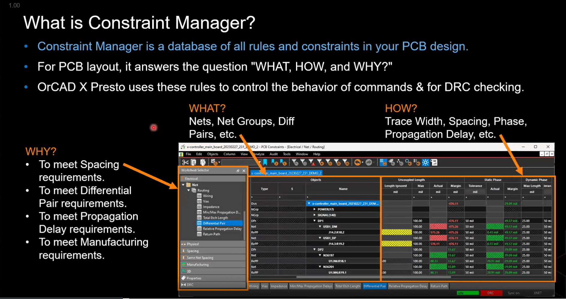
The Constraint Manager in OrCAD X can help implement and enforce impedance, lane width, pair spacing, and backdrilling rules, ensuring that the backplane meets each communication standard's signal integrity and performance requirements.
Routing Guidelines for High-Speed Backplane Design
|
Standard |
Impedance |
Lane Width |
Pair Spacing |
Backdrilling |
Skew Matching |
Topology |
|
PCIe Gen 5/6 |
85Ω differential |
4.5 mils |
10 mils |
Required |
<2 ps (PCIe Gen 6 PAM4) |
Point-to-Point (Switched Fabric) |
|
Ethernet 100G/400G |
100Ω differential |
6 mils |
12 mils |
Required for 10G+ |
<3 ps for 100G Ethernet |
Switched Network (Layered) |
|
InfiniBand HDR/NDR |
100Ω differential |
6-7 mils |
15 mils |
Required for 50G+ |
<1.5 ps |
Switched Fabric |
|
VPX (PCIe/RapidIO-based) |
85Ω (PCIe), 100Ω (Ethernet, RapidIO) |
4.5-6 mils |
10-12 mils |
Required |
Tighter for VPX PCIe, less for RapidIO |
Modular / Mesh / Star |
|
RapidIO Gen 3/4 |
100Ω differential |
5-6 mils |
10-15 mils |
Lower impact at ≤10G |
<5 ps |
Deterministic Packet-Switched |
How OrCAD X Enables High-Speed Backplane Design
|
OrCAD X Features |
How It Aids in High-Speed Backplane Design |
|
Ensures impedance control, trace width, and spacing, meeting high-speed design standards. |
|
|
Flags violations like incorrect trace width and spacing, preventing issues such as signal reflections and crosstalk. |
|
|
Optimizes impedance (e.g., 50Ω or 85Ω) to meet design specifications, ensuring signal integrity by adjusting trace widths for different stack-ups and material properties. |
|
| Signal Integrity Analysis |
Detects coupling (e.g., >10% coupling), impedance mismatches, and skew issues, allowing early resolution of signal integrity issues. |
| 3D Visualization |
Visualizes the layout, ensuring proper routing of differential pairs and minimizing mechanical issues such as via length or ground plane alignment. |
With OrCAD X, ensure your high-speed backplane design meets signal integrity, power, and manufacturability requirements. Explore how the OrCAD X platform can optimize the high-speed backplane design process, with a free trial today!
Leading electronics providers rely on Cadence products to optimize power, space, and energy needs for a wide variety of market applications. To learn more about our innovative solutions, subscribe to our newsletter or our YouTube channel.