Via Stitching in OrCAD X: Enhancing Design Performance
Key Takeaways
-
Via stitching creates a continuous grounding system, reducing electromagnetic interference.
-
Use via stitching to create EMC rings around board edges and distribute vias across the board shape for better signal integrity and EMI reduction.
-
Utilize OrCAD X via array tool for efficient via placement, ensuring proper grounding and compliance with EMC regulations.
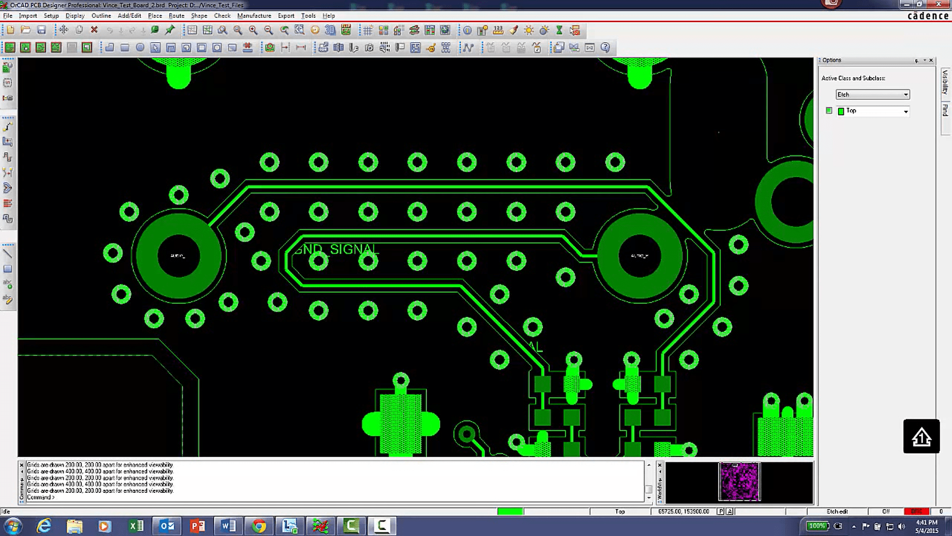
Via stitching around a trace and pads in OrCAD X.
Via stitching in PCB design improves electrical performance and mechanical stability. Via stitching involves placing multiple vias in a grid-like pattern across an area of a PCB, notably around the edges of ground planes, power planes, and signal traces.
Via Stitching: Purpose and Benefits
|
Purpose |
Benefit |
|
EMI Reduction |
Creates a more continuous grounding system, reducing electromagnetic interference. |
|
Signal Integrity Improvement |
Maintains a consistent reference plane for high-speed signals, minimizing noise and crosstalk. |
|
Thermal Management |
Spreads heat more evenly across the PCB, improving thermal management. |
|
Mechanical Strength |
Increases the mechanical strength of the PCB, especially around connectors and mounting holes. |
|
Power Distribution |
Improves power distribution by creating multiple parallel paths for current flow. |
|
Ground Loops Minimization |
Minimizes ground loops by ensuring the ground plane is well connected throughout the PCB. |

Preview of via array around the board edge for EMI reduction.
Examples Using Stitching Vias
Via stitching and via arrays are similar and oftentimes applied to the board using the same tool. However, there are slight differences.
-
Via arrays are structured groupings of vias used for high-density interconnections, thermal management, and mechanical support, typically beneath components like BGAs.
-
Via stitching involves placing vias along ground or power planes to reduce EMI and improve signal integrity by providing continuous grounding paths.
Example 1: EMC Ring Around the Edge of the Board
Adding stitching vias around the edge of the board to create an EMC (Electromagnetic Compatibility) ring helps to prevent electromagnetic interference (EMI). An advanced PCB software has a "surrounding" option for creating via arrays, in addition to specifying distance from the board edge. Through this method, vias can be placed at regular intervals along the perimeter.
This configuration provides a continuous grounding path, acting as a shield to contain EMI within the board and block external electromagnetic fields. This method is crucial for meeting EMC regulations and ensuring reliable board operation in noisy environments.
Example 2: Stitching Vias Across a Whole Shape
Distributing stitching vias across the entire shape of the board improves signal integrity and reduces electromagnetic interference. By selecting a "across-board" or "across-shape" option in your software via array command, vias can be evenly placed across the designated area.
This technique ensures robust interconnection of ground planes, maintaining a consistent ground reference and minimizing the loop area for high-frequency currents. This is particularly important for high-speed designs and sensitive analog circuitry, as it reduces radiated emissions and susceptibility to external noise, thereby preserving signal quality.
Working With Via Stitching in OrCAD X
Via arrays are used to quickly add groups of vias for various purposes, such as creating EMC rings around the board's edge, RF screening vias, or stitching vias across a shape or section of the board. Some tips to keep in mind when working with via stitching in OrCAD X include:
-
Preview Adjustments: Utilize the preview feature to make the necessary adjustments before finalizing.
-
DRC Enabling: Keep DRC enabled to automatically resolve any violations and ensure compliant designs.
-
Parameter Tweaking: Adjust via parameters such as distance and offset to achieve the desired electrical and mechanical properties.
Placing Via Stitching Using the Via Arrays Tool in OrCAD X
|
Step |
Description |
|
Accessing Via Arrays |
Use the Place > Via Array command. Ensure that the options panel is accessible for adjustments. |
|
Settings Overview |
|
|
Define Via Parameters |
|
|
Choose Array Options |
|
Enhance your PCB design with effective via stitching using OrCAD X. Leverage advanced features to improve EMI reduction, signal integrity, and thermal management in your designs. Explore our PCB Design and Analysis Software and discover the powerful capabilities of OrCAD X for your next project.
Leading electronics providers rely on Cadence products to optimize power, space, and energy needs for a wide variety of market applications. To learn more about our innovative solutions, talk to our team of experts or subscribe to our YouTube channel.