Using Dimensions in OrCAD X for Manufacturing Accuracy
Key Takeaways
-
Dimensioning is vital to capture component manufacturer accuracy/precision when creating footprints.
-
The board layout uses a customizable grid where users can select between units (mils/mm/microns) and interval steps.
-
Live DOC offers an easy-to-use linear, ordinate, and radial dimensioning tool.
It’s easy to communicate fabrication/placement guidelines to manufacturers using dimensions in OrCAD X.
Manufacturing depends on the accuracy of the project’s physical dimensions; PCB product development has many design stages where adherence to dimensioning is critical. Without careful consideration of how dimensioning translates to the design and manufacturing equipment, production can require considerable revisions, defect proliferation, or an overall reduction in yield that swells costs.
When using dimensions in OrCAD X—whether from manufacturers' datasheets or internal design documents—consider the following features and design guidelines to ensure a successful PCB production.
Dimensioning During PCB Design
|
Footprint Creation |
|
|
Layout Grid |
|
|
Manufacturing Outputs |
|
Capturing Component Dimensions Accurately
There are two general stages of dimensioning to consider when designing PCBs. First, components: manufacturers provide dimensioning in either metric as millimeters (mm) or Imperial as thousands of an inch (mils). Designers should always use the exact units stated by the manufacturer in the datasheet and avoid conversions (even conversions given by the manufacturer) to prevent rounding errors that can accumulate within a design and lead to board fabrication and assembly defects.
There is a slight advantage when working with mils as a mil is exactly 0.0254 mm while a mm is approximately 39.3701 mils; informally, designers can use a 1:40 mm-to-mil conversion factor to check units, but this should only be for ballparking measurements, never for actual manufacturing specs. Component pin pitches were historically defined in units of mils (as were other aspects of board manufacturing like thickness, plating, etc.); manufacturers are more likely to express measurements in their dominant measurement system these days. Depending on the components selected for the circuit, it’s common for an assembly to contain both footprint types (designed in mils or mm).
Design teams wishing to sidestep potential issues owing to component packaging dimensioning can instead use the footprints of trusted data vendors through the Component Explorer in OrCAD X Capture. Beyond ensuring the component dimensioning is correct, footprints will include all the necessary supporting models (schematic and PSpice symbols, 3D body, etc.) for a comprehensive component library management solution.
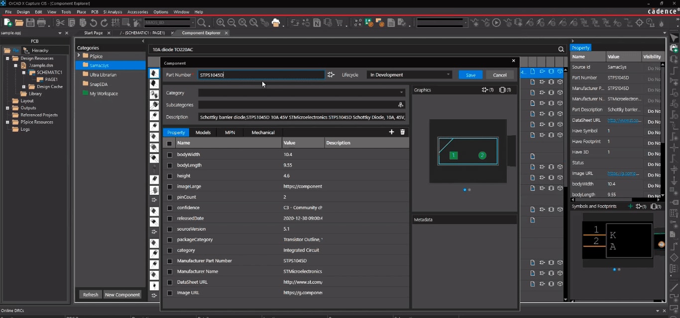
Design teams can use trusted data vendors for footprint sourcing.
Using Dimensions in OrCAD X Presto PCB Editor
Once PCB design moves to the board layout environment, designers can specify whether they want their grid to be in mils, mm, or microns (since a micron is just a mm-hundredth, we’ll ignore the unit for this discussion). The grid defines the smallest step possible between on-grid points for both planar axes.
For example, consider a .25 mm-square grid (a grid point in both XY directions every .25 mm): to remain on-grid, two identical 1005 (1 mm length, 0.5 mm width) chip packages with footprint lengths of 1.9 mm and grid snap points at the component center can have a minimum place bound edge clearance of 0.10 mm in a “series” configuration. However, if the grid point spacing is .025 mm instead, the nearest place bound lines of the two components can be coincident because of the smaller on-grid point intervals.

Designers can set grid units and intervals for more accurate layouts.
Why not always use the smallest possible grid intervals to maximize placement density? Extremely compact placements can overly constrain manufacturing, leading to lower yields and the potential for more defects. Especially when manufacturing for moderate-to-high volume quantities where cost and yield become the dominant criteria for a successful design, giving the manufacturer additional leeway (when available) can improve production outcomes. For prototyping (especially HDI boards), designers can get away with tighter placements as the low-volume nature and evolving design mean any thermal/electrical/mechanical issues stemming from the tight placement can be overcome in the next revision. When in doubt, follow the manufacturer’s datasheet recommendations for spacing around high-power/high-current components (power ICs, SMPS inductors, etc.) and avoid placing components too close to connectors, test points, mounting holes, and other board features that require a tool or hand access.
Designers must include dimensions on the relevant files when producing manufacturing artwork to assist the manufacturer. Fortunately, the new Live DOC feature makes it easy to do so. Designers can right-click on the dimensioning tool to select from linear, ordinate, and radial dimensioning features. With Live DOC, designers never have to worry about their manufacturing documentation being out-of-date with the most recent updates to the board file – Live DOC updates always synchronize with the board file, so any changes made to the board file show up instantaneously in Live DOC.
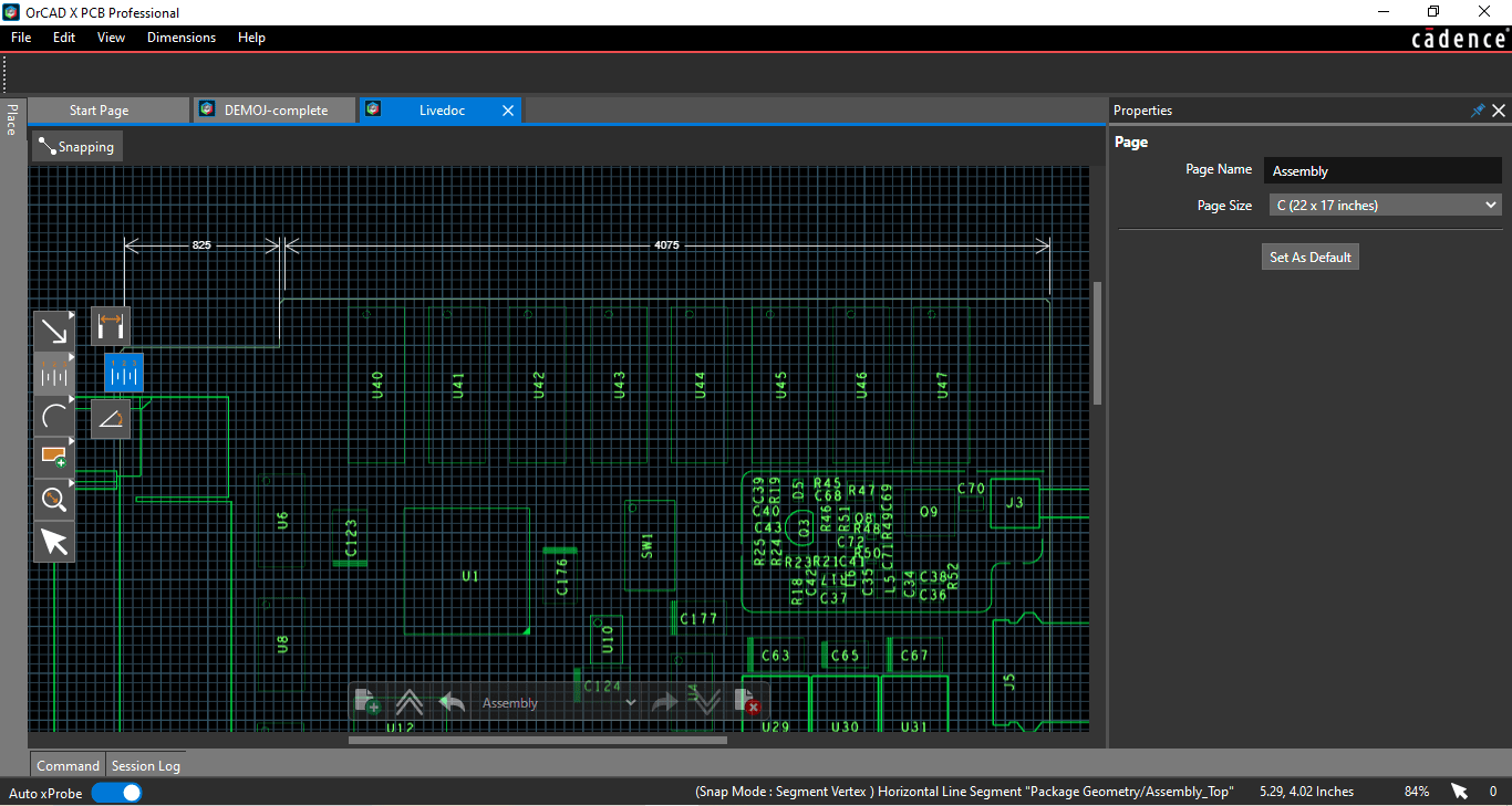
Designers can quickly select between different dimensioning types in Live DOC.
Cadence Design for Manufacturing Solutions
Using dimensions in OrCAD X is crucial to communicating the project's design intent; without accurate dimensioning, designs can suffer unplanned revisions after entering production, draining design team resources. By getting ahead of manufacturing requirements at the outset of a design, PCB project teams can ensure a seamless transition to manufacturing after layout that keeps project budgets and timelines on target.
For every stage of PCB design, the new OrCAD X platform makes it easy for design teams to accelerate product development with powerful and easy-to-use tools. Interested in learning more? See how Cadence PCB Design and Analysis Software simplifies design for manufacturing.
Leading electronics providers rely on Cadence products to optimize power, space, and energy needs for a wide variety of market applications. To learn more about our innovative solutions, talk to our team of experts or subscribe to our YouTube channel.