Schematic to PCB Layout
Key Takeaways
-
Before starting the PCB layout process, ensure your schematic is free of design rule violations to avoid conversion issues.
-
Begin with setting up your workspace, defining the board's dimensions, and choosing the appropriate materials and layer types.
-
Employ EDA software effectively to facilitate the schematic to PCB conversion, set constraints, and perform Design Rule Checks (DRC).
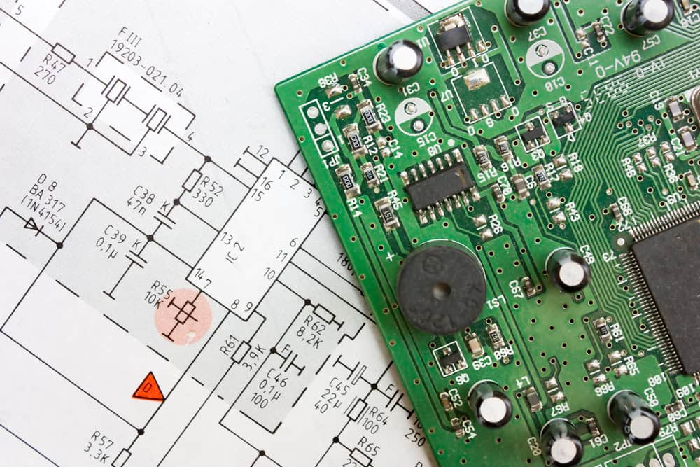
Schematic to PCB layout is a major step in the creation of circuit boards.
Transitioning from a schematic to a PCB layout marks a major step in the development of circuit boards, involving the transformation of a circuit diagram into the physical layout. Despite the complexity of the process, the fundamental steps of data transfer from schematic to circuit board remain consistent, ensuring that creating a PCB layout from a schematic doesn't have to be a daunting task.
Schematic to PCB Layout Steps
|
Step |
Step Description |
|
Verify that the schematic is free from design rule violations to ensure a smooth transition to PCB layout. |
|
Define the grid, origin, board dimensions, and layer materials and types. Consult with your CM for optimal dimensions and materials to reduce waste and cost. |
|
Use ECAD software to scan for schematic errors, generate a netlist, and guide the transition to a board layout with component placement considerations. |
|
Place components, traces, vias, and copper pours, adhering to spacing and clearance guidelines for manufacturability and functionality. |
|
|
Conduct a Design Rule Check to ensure adherence to design rules and CM’s DFM guidelines, optimizing the design for manufacturing. |
Schematic to PCB Layout Process: Schematic Check
The transformation of a schematic into a PCB can be done in your ECAD software, allowing for a smooth transition. Ensure your schematic is free from design rule violations that could hinder its conversion into your PCB layout. Your EDA software should flag any errors, such as unconnected wires, floating nodes, and more, depending on your design and configuration.
Configuring Layout: Board and Stackup
Initially, it's important to establish your workspace in your layout editor to suit your board’s needs:
- Define the appropriate grid and origin for your layout.
- Create (or modify) the board outline to match the required dimensions of your device. Most ECAD tools provide a selection of default board sizes, including various area dimensions and thickness options. However, consulting with your Contract Manufacturer (CM) prior to selection is recommended, as certain board dimensions might lead to unnecessary material waste, escalating manufacturing expenses.
- Specify the materials for the board, as well as the number and types of layers needed for your design.
Transferring the Schematic Over
Many ECAD software packages offer a feature that scans for errors within your schematic, generates a netlist, and facilitates the transition of your schematic into a board layout, often employing a wizard to guide you through the process step by step. Following this, positioning the components on the board is the subsequent phase, where adhering to specific spacing and clearance guidelines is critical to ensure the manufacturability of your board.
Layout and Routing
After conversion, you'll be greeted with component footprints defined in your schematic and electrical connections that are yet to be transformed into physical connections on the board. The PCB designer's job is to place these components, lay out traces and vias, then place copper pours as needed. Trace routing is a particularly demanding aspect of PCB layout, especially for complex multilayer boards featuring numerous vias. It's also crucial to adhere to specific spacing and clearance standards during the trace routing process to ensure the board's functionality and manufacturability.
DRCs and Validation
Before sending your PCB design to fabrication, ensure your design has been checked for any potential errors. Following the steps outlined, after completing the layout and routing stage, your board will be ready for a thorough examination and adjustment of components, copper configurations, and collaborations between ECAD/MCAD design teams, as well as addressing procurement needs. This involves conducting a Design Rule Check (DRC) analysis to verify adherence to the predefined design rules and constraints. Furthermore, aligning these rules with your Contract Manufacturer's (CM) Design for Manufacturability (DFM) guidelines is essential to guarantee that your design is optimized for successful manufacturing.
Your EDA Software’s Role in the Process
The process of converting from a schematic to PCB layout is largely determined by your EDA software. For this reason, using EDA software that can guide you in the conversion process is critical. It’s important that before laying out your board, you ensure that you have the correct grid spacing, constraints, and any other rules set up.
Defining Constraints in OrCAD X and DFM
In OrCAD X, you can establish spacing and physical design rules using the Constraint Manager for efficient routing. Accessed via Tools, it provides a comprehensive overview of electrical and physical constraints. Within the Physical Constraint Set, users can create custom constraint sets, such as for power nets, and define parameters like line width and neck length. These settings are flexible, allowing adjustments for different layers and automatically propagating changes downward. Furthermore, users can easily apply these constraints to specific nets, ensuring uniformity and efficiency in design.
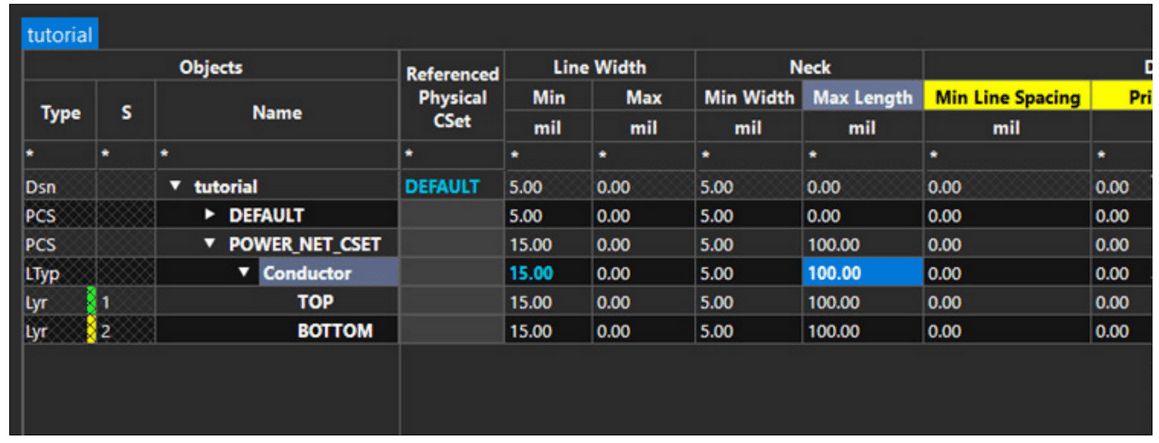
Changing the Neck Length in OrCAD X constraint manager
OrCAD X offers a suite of powerful Design for Manufacturing (DFM) checks, accessible through the Manufacturing worksheet in the Constraint Manager. They cover a wide range of advanced constraints including mask, copper, and silkscreen checks. Specific features include Package-to-Package Spacing checks for organizing components into specific classes and enforcing distinct spacings. Via Under Component constraints ensure vias are appropriately positioned, while checks for Through-hole pins under SMD components identify potential placement hindrances
Setting Up Grids in OrCAD X
Grids help control component placement by establishing a regular spacing pattern between components in horizontal and vertical directions. Routing operations also require grids to place connections at the grid points.
Specific grid spacing can easily be set up in OrCAD X by clicking the #Grids icon from the top-left corner of the design canvas to view the grids widget. The widget displays grid values in Mils, MM, and Microns.
Click the On button in the Visibility section to enable grids, you can select any predefined grid value or enter a custom value into the Quick Grid x/y fields if you need a custom or non-uniform grid. The modified grid values are applied globally and used for subsequent routing or placement operations. However, this change does not affect placed components or existing connections and vias.
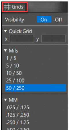
Grid setup in OrCAD X Presto PCB Editor
Experience the power of seamless design transitions, sophisticated layout capabilities, and comprehensive validation tools. Try OrCAD X with our free trial.
Leading electronics providers rely on Cadence products to optimize power, space, and energy needs for a wide variety of market applications. To learn more about our innovative solutions, talk to our team of experts or subscribe to our YouTube channel.
Leading electronics providers rely on Cadence products to optimize power, space, and energy needs for a wide variety of market applications. To learn more about our innovative solutions, talk to our team of experts or subscribe to our YouTube channel.