MIPI PCB Design Guidelines for High-Speed Interfaces
Key Takeaways
-
Differential Pair Routing: Maintain controlled impedance and continuous ground reference planes to reduce noise and ensure signal integrity.
-
Implement solid ground planes, via stitching, and proper shielding to enhance grounding and minimize electromagnetic interference.
-
Keep within-pair length differences ≤ 5 mils and between-pair mismatches ≤ 50 mils to prevent timing issues.

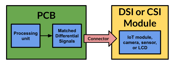
Simple diagram of MIPI PCB design.
The MIPI PCB signaling standards have become widespread in computers, networking equipment, smart electronics, and other fields. They are crucial for enabling high data rates while maintaining relative immunity to noise.
There are a couple of major standards depending on your desired interface module. The Camera Serial Interface (CSI), Display Serial Interface (DSI), and PHY (Physical Layer) Design Guidelines are all integral components of MIPI standards, each serving a specific purpose in ensuring efficient, high-speed communication between components. Read on as we delve into each, and cover important MIPI PCB design guidelines.
Basic MIPI PCB Design Guidelines
|
Category |
Guideline |
|
|
|
Length Matching |
|
|
Minimize Crosstalk |
|
|
Grounding |
|
|
Layer Stackup |
|
|
Via Management |
|
|
Power Supply |
|
|
EMI and Signal Integrity |
|
|
Thermal Management |
|
Camera Serial Interface (CSI) Design
The MIPI CSI interface is primarily used for camera modules in mobile devices. CSI can be adjusted to accommodate different resolutions and frame rates, making it ideal for a wide range of applications, from basic webcams to high-definition cameras in smartphones. Both CSI and DSI depend on the PHY design to guarantee efficient and reliable high-speed data transfer.
Key guidelines for CSI design include maintaining a differential signal line topology for transmitting data (Tx) and receiving data (Rx), ensuring differential impedance of 100Ω ± 20%, and keeping line lengths as short and equal as possible to minimize skew and signal degradation.
Use continuous ground planes and ground vias to ensure robust signal integrity. Power line topology guidelines for CSI emphasize low resistance (≤ 30mΩ) and inductance (≤ 2.8nH/5ch), with capacitors placed close to the package pins to minimize ripple noise and enhance power stability.
Display Serial Interface (DSI)
The MIPI DSI interface is designed for display modules in mobile and embedded devices. It supports high-resolution and high-refresh-rate displays. DSI enables the transmission of high-quality graphics and video, ensuring smooth and superior display performance.
The Display Serial Interface (DSI) design within the MIPI (Mobile Industry Processor Interface) standards ensures efficient, high-speed data transfer between display modules and host processors. DSI utilizes a differential signal line topology for both transmission (Tx) and reception (Rx), adhering to a differential impedance of 100Ω ± 20%.
Designers should aim to minimize line length differences and maintain line lengths as short and equal as possible. Proper line spacing, especially a minimum of three times the spacing (3S) between differential pairs and adjacent signals, is crucial to reduce electromagnetic interference and crosstalk.
For power line topology, DSI requires low resistance (≤ 30mΩ) and inductance (≤ 2.8nH/5ch) in the PCB design, with capacitors placed near the package pins to minimize ripple noise and maintain stable power supply -(MIPI PCB)-.
MIPI PHY Design Guidelines
MIPI (Mobile Industry Processor Interface) PHY defines the physical layer specifications for various MIPI interfaces, including D-PHY, C-PHY, and M-PHY. These PHY layers are crucial for high-speed data transmission. The PHY (Physical Layer) design guidelines for MIPI are crucial for ensuring reliable high-speed data transfer.
MIPI standards include three primary PHY layers: D-PHY, C-PHY, and M-PHY, each tailored for specific applications:
-
MIPI M-PHY: Designed for data-intensive applications such as transferring high-resolution images, high-frame-rate video, and data transfer between mobile displays and memory. It is also used in mobile communications and storage.
-
MIPI D-PHY: Commonly used in smartphone cameras and displays, providing high-speed communication between the device and its processor. It is also utilized in automotive systems, including radar, cameras, infotainment systems, and dashboard displays.
Both M-PHY and D-PHY use typical differential signaling, but with different clocking methods. D-PHY uses a source-synchronous clock, while M-PHY uses an embedded clock.
-
MIPI C-PHY: Initially created for mobile cameras and displays, it is now also used in wearables, IoT camera systems, and automotive displays/cameras. C-PHY can share the same physical layer and device pins as D-PHY, allowing designers to use a system-on-chip (SoC) that operates in both modes. MIPI C-PHY Utilizes a more complex differential signaling scheme with three pins per lane, employing three signal levels sensed differentially, similar to bipolar-return-to-zero (bipolar-RZ). This scheme requires 50 Ohm characteristic impedance for each line and 100 Ohm differential impedance between lines, with a total of three lanes. These differential lines must be length-matched on the PCB to ensure that the rising edges coincide, accurately detecting signal levels and suppressing common mode noise.
MIPI PHY design guidelines include ensuring equal lengths for both differential pairs to reduce signal skew and degradation. It’s best to maintain a minimum of three times the spacing (3S) between differential pairs and adjacent signals, to mitigate electromagnetic interference and crosstalk
Overall, these guidelines ensure that various sensors, imaging components, peripherals, and SoCs can effectively communicate and operate across different interfaces by leveraging the appropriate physical layer for their applications.
Implementing MIPI PCB design guidelines is essential to ensure high-speed data transfer in PCBs. With Cadence tools, specifically the OrCAD X platform, designers can efficiently manage the complexities of MIPI interface designs.
Cadence’s PCB Design and Analysis Software —specifically the OrCAD X platform, aids in adhering to these guidelines. Through specialized tools like the constraint manager, you can create custom rules and ensure that you follow MIPI PCB design guidelines.