Better PCB Design Using OrCAD X
Key Takeaways
-
OrCAD X users can utilize powerful visibility and filter tools to hone in on the design.
-
Constraint-driven placement and routing tools ensure designs remain manufacturable without requiring revisions.
-
Manufacturing and MCAD integration benefits from a 3D viewer and synchronized-to-design documentation.
Designers can experience better PCB design using OrCAD X.
Depending on the team and project size, PCB designers sometimes wear many hats when translating schematic pages into board file documentation for manufacturing. From stackups and impedance structures to footprints and constraint management, the devil can be in the details, and when budgets and timelines are tight, board designs have little room for error. Fortunately for designers and small project teams, OrCAD X is here to help with a bevy of new features that make PCB design using OrCAD X easier than ever.
Improving PCB Design Using OrCAD X Features
|
Live BOM |
Using up-to-date data from Sourcengine, examine a BOM's risk profile, search for replacement components, and monitor the supply chain. |
|
Live DOC |
Synchronized manufacturing documentation ensures that project outputs always reflect the most recent changes. |
|
Workspaces |
Collaborate online with design team members; administrators can set view/edit privileges for files to maintain file integrity. |
Preparation and Setup for PCB Design Using OrCAD X
The circuit board layout starts with the schematic, and incorporating these symbols into the layout (through netlisting) requires footprints. Librarians or designers must generate footprints (when they conform to IPC standards), build from scratch, or use a third-party vendor for verified footprints. When footprints are complete, open up the property editor for the schematic and enter the PCB footprint names for each component.
The first thing to do in OrCAD X Presto PCB Editor is to set up the different available design parameters. OrCAD X allows users to customize the environment to their needs and tastes. For instance, OrCAD X users can either display or hide the net names on design objects in the display. Other adjustable parameters include colors, units, text, grids, and other display preferences.
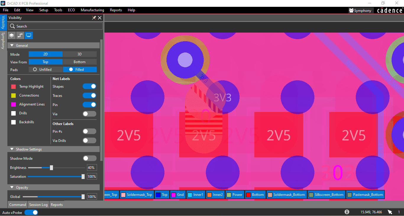
The OrCAD X Presto PCB Editor Visibility panel supports numerous view configurations.
The last part of setting up the layout design is creating its physical characteristics, starting with the board outline. Users can define the board outline and other notable design features in OrCAD X Presto PCB Editor, like slots or board cutouts, by specifying the shape coordinates. The Cross Section Editor will generate the board layer stackup, where users can define the materials and thicknesses of the board's conductor and dielectric layers. Finally, users will input design rules and constraints using the Constraint Manager. OrCAD X Presto PCB Editor also allows you to import all of this data to leverage work done in other systems or by vendors.
Placement Options
The first part of placing components on the board is working with parts that are not part of the netlist. These include tooling, mounting holes, or other mechanical parts that aren’t connected electrically. As you can see in the picture below, the placement tools specify a mounting hole that the designer can locate either by entering the desired coordinates or placing it manually with the mouse.
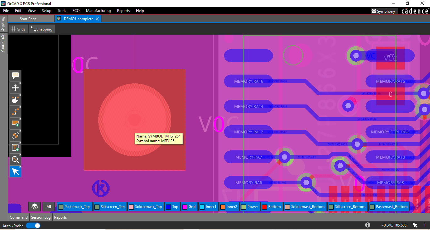
A mounting hole near the board edge, as shown in OrCAD X Presto PCB Editor.
The next step is to place all the electrical components on the board using the same functionality. Users can quickly place, align, shift, rotate, and flip components between board sides. Another handy feature is to set up the schematic for cross-probing with the layout. This way, you can select the parts you want to place in the schematic, which the system highlights for grouping within the layout.
Easy-to-Use Layout Tools
OrCAD X Presto PCB Editor gives designers plenty of capabilities when routing traces. You can go into the manual routing mode, select a net, and route it as a trace. While routing the trace, you can maneuver it around, pushing and shoving other traces out of the way. You can also select a previously routed trace and use the slide command to move it around, pushing and shoving other traces out of the way. Here, the importance of setting up design rules and constraints becomes evident as you work with the different trace widths, spacings, and vias of the nets to complete your routing as desired.
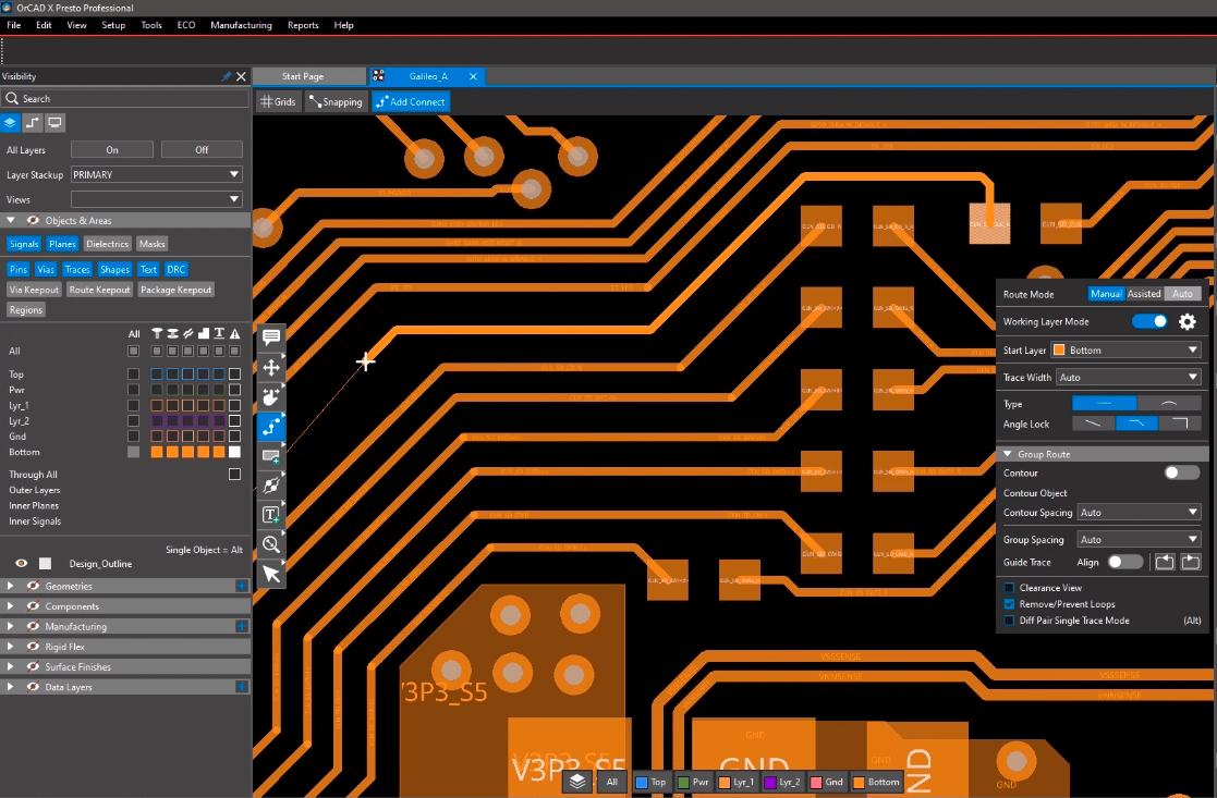
Interactive and intuitive routing features make the layout a breeze in OrCAD X Presto PCB Editor.
Another part of routing is working with the power and ground nets in the design. While it’s possible to route them with wider traces – thanks again to the specific design rules set up for them – they often require dedicated power and ground planes. OrCAD X Presto PCB Editor gives designers many options for creating, configuring, and connecting reference plane layers. With the design rules set up in the constraint manager, the online DRCs provide constant, live feedback while designers place and route the board. However, at the end of the design, it is always a good practice to run one last check to ensure the board is completely ready for manufacturing. OrCAD X has expansive 3D capabilities, allowing design teams to check the board for clearance errors in mechanical objects and helping to display the board for design reviews, including flex and rigid-flex connectors.
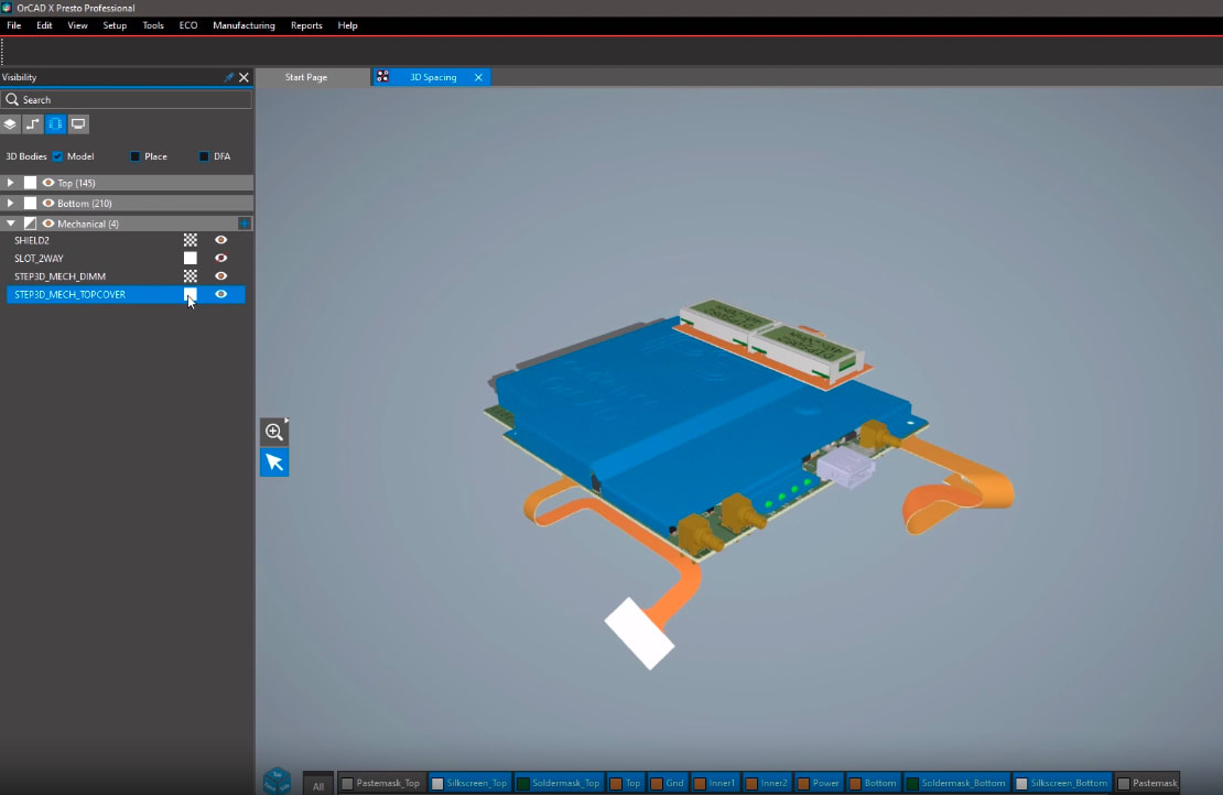
Interactive and intuitive routing features make the layout a breeze in OrCAD X Presto PCB Editor.
Manufacturing Outputs for Seamless Productions
Now that the board placement and routing are complete, it is time to prepare it for manufacturing. OrCAD X Presto PCB Editor has many features that help designers. Live DOC makes managing artwork easier than ever with a live-linked template synchronizing documentation and design. OrCAD X gives designers many different tools to create and bundle together the various fabrication and assembly files required by a manufacturer, and another option is available here as well. Designers can use the IPC-2581 export functionality to create a fully encapsulated manufacturing database for direct-to-vendor communications. This format allows users to exchange information back and forth with your manufacturers to ensure complete design integrity.
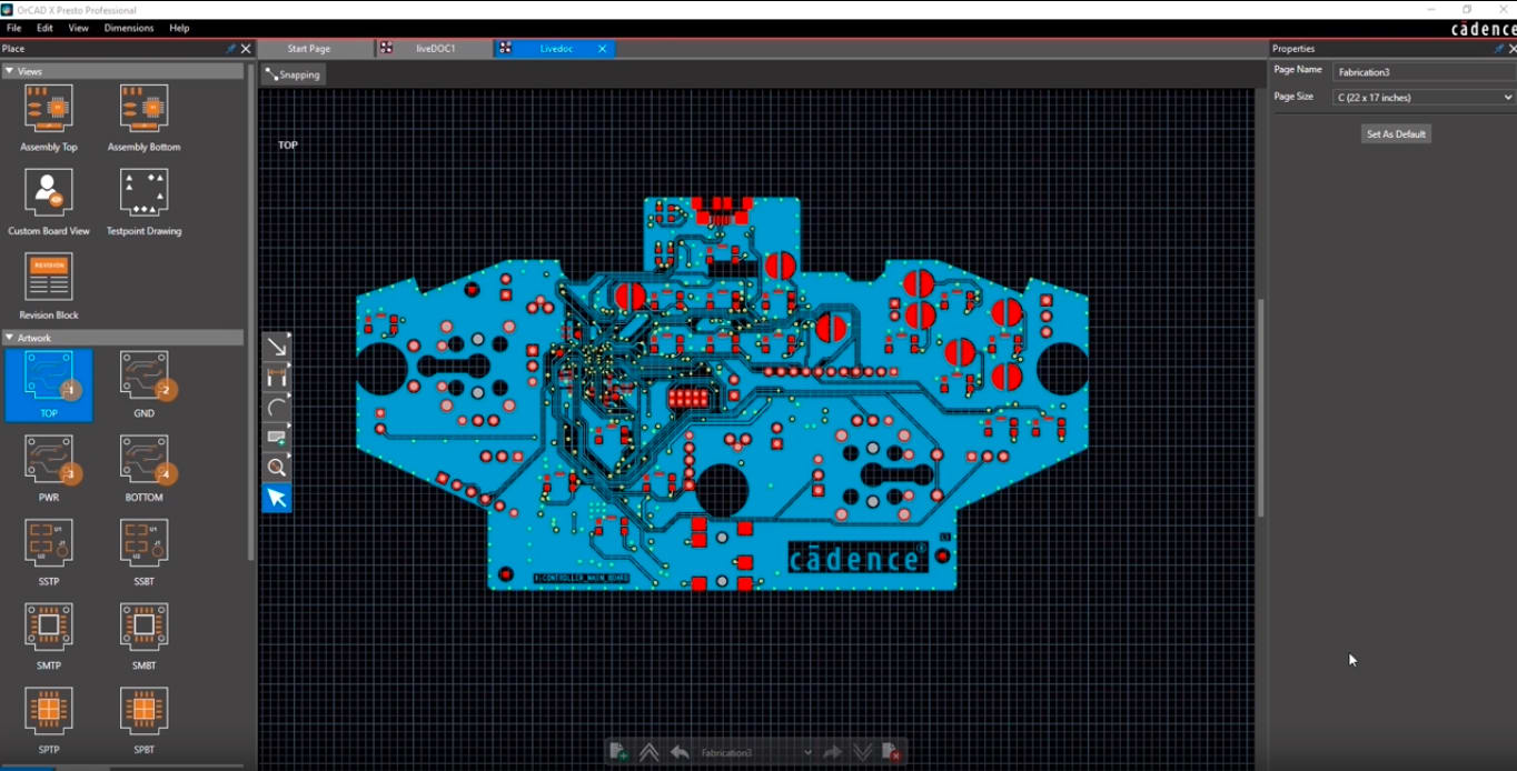
Live DOC in OrCAD X Presto PCB Editor synchronizes design and documentation.
Cadence Solutions for Modern (and Future) Electronic Design
For electronics development, PCB design using OrCAD X helps design teams realize cutting-edge projects with an easy-to-use toolset. New features like Live BOM and Live DOC make it easier to translate schematics and layouts to readily manufacturable outputs. Along with the powerful PSpice simulation tool, design teams can fully anticipate performance before prototyping. Interested in learning more? See how Cadence PCB Design and Analysis Software is helping deliver the future of electronic design.
Leading electronics providers rely on Cadence products to optimize power, space, and energy needs for a wide variety of market applications. To learn more about our innovative solutions, talk to our team of experts or subscribe to our YouTube channel.