Optimization Guide for PCB Design Constraints
Key Takeaways
-
The problems that can happen by not using constraints with your PCB routing.
-
The different types of PCB routing constraints you can work with in your design.
-
How to apply rules and constraints to your PCB routing.
Complex PCB routing requires rules and constraints for success.
As PCB designers, setting up rules and PCB design constraints for routing a printed circuit board is a critical part of our job. It can take time and involve research and manual input, but setting up these constraints and routing your board according to the rules can save your design from ending in disaster. We’re going to examine some of the reasons why PCB routing constraints are important and then show how using them can add a lot of value to your next design —specifically with OrCAD X.

Problems With Not Using Rules and PCB Design Constraints in Routing
Constraints and rules will help you to organize your design and communicate important information between the schematic and the layout. Primarily, though, they are used to prevent manufacturing problems and to ensure the electrical performance of the circuit board. Here are some issues that constraints are designed to address:
Manufacturing Problems:
Components that are placed too close to each other or oriented incorrectly may be difficult to assemble or solder correctly. Additionally, auto-insertion machinery may not be able to place the parts as needed, and technicians doing manual assembly may not be able to fit their tools and solder materials into the tight areas. The closer those parts are to each other, the more potential for collateral damage, as hot soldering irons or other tools impact nearby components.
Metal on the circuit board that is too close to other metal objects may also cause problems during the manufacturing process. Solder slivers can form, causing intermittent shorts, which are difficult to find and correct. Solder can also bridge between traces or pads causing direct shorts. Parts that are connected to large areas of metal, such as small surface-mount bypass capacitors attached to a ground plane, may not solder correctly without the correct thermal reliefs.
Electrical Performance:
Traces used to conduct power that aren’t wide enough may be inadequate for the amount of current they carry. Some traces also must have exact widths to control their impedance. Other traces need to be routed to a specific length or to match the length of similar nets. Differential pairs must be perfectly routed side-by-side. Still, other traces may need to be routed in specific patterns or “topologies.” All traces may or may not have spacing requirements to other traces side by side, above, or below them.
It used to be that you could take a PCB design, throw it into the auto-router, and end up with a completely routed board that worked perfectly. That is no longer the case. Without the proper care in trace routing widths, spacing, lengths, and topologies, you may end up with a plethora of signal integrity problems. These can range from crosstalk, reflections, ground bounce, and electromagnetic interference.
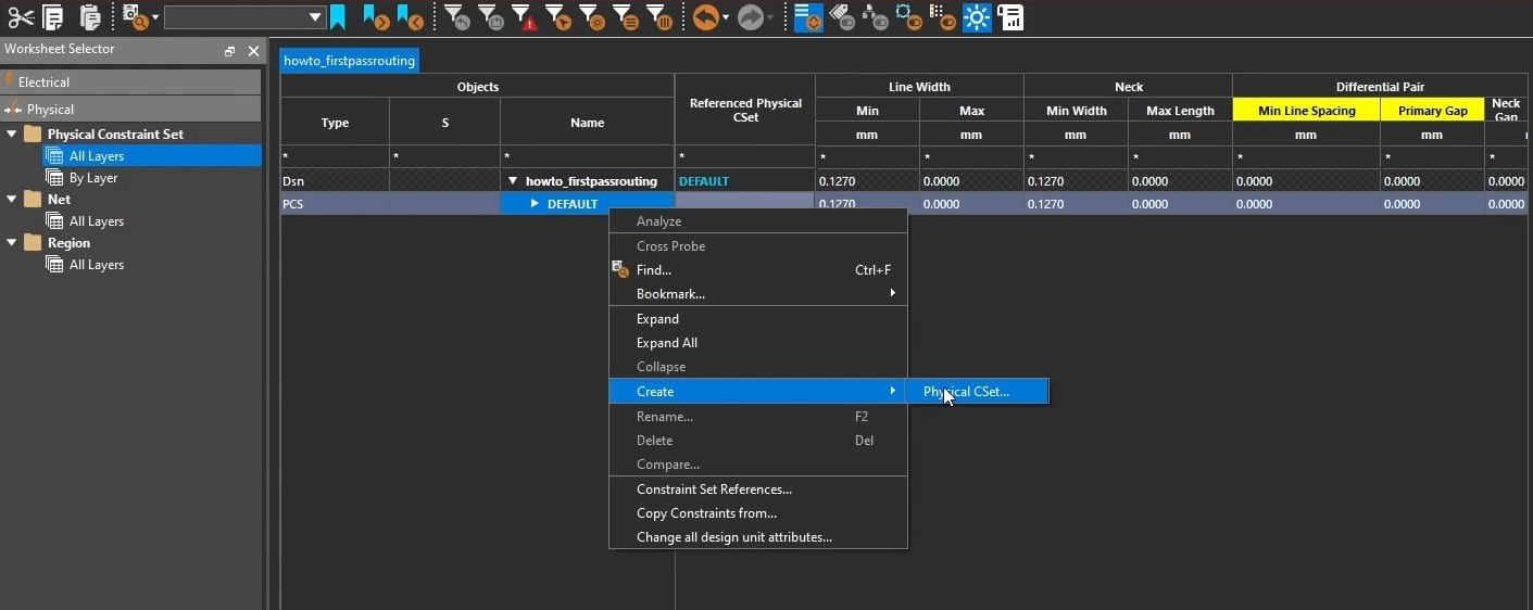
Through the OrCAD X constraint manager, CSETS are applied to different nets or regions in the design. The image shows how to create a new CSET.
What Are the Different PCB Routing Constraints?
There are many different rules and constraints that you can set up for routing your PCB design, and we will list some of them here as examples. We’ll start with some non-routing constraints on components because even those will ultimately have an effect on your routing.
|
Constraint Category |
Description |
|
Components |
- Set clearances to other parts or objects and board outline features such as cutouts. |
|
Trace Widths |
- Set default widths for most nets in a design, or specify widths for particular nets or net classes. |
|
Trace Clearances |
- Control clearances for trace-to-trace, trace-to-pad, trace-to-via, trace-to-other metal, and trace-to-other features (e.g., drill holes or board edges). |
|
Trace Routing |
- Apply minimum and maximum length constraints for traces. |
|
Vias |
- Specify types of vias used for individual nets or net classes, including thru-hole, blind, buried, and microvias. |
|
Planes |
- Manage how power and ground planes connect to traces and components with thermal reliefs. |
These are just some of the constraints that you can work with to help your PCB routing. The next step is to add these constraints to your design.
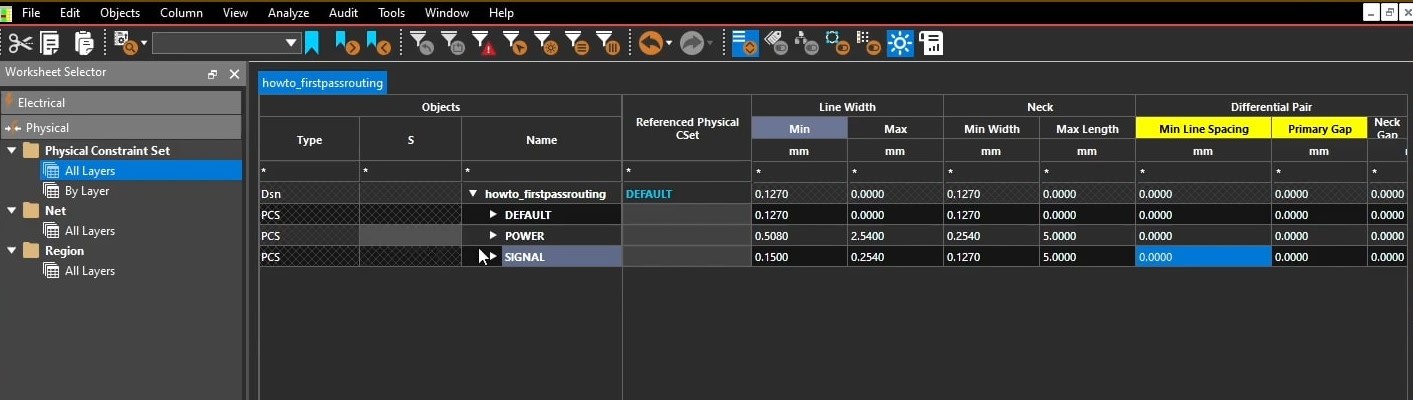
Two physical CSETS for power and signal. Yellow column headers mean the rule is off, and can be changed by right-clicking on it.
Getting Started With OrCAD X: Design Tips for Setting Up Rules and PCB Constraints
In OrCAD X, you can set up design constraints and rules for PCB routing directly from either the schematic or layout, providing flexibility across the design process. With OrCAD X, the Constraint Manager is the central tool for managing all these rules, from trace widths to spacing. Early constraint setup minimizes errors, helps to ensure signal integrity, and addresses manufacturing requirements proactively. In the OrCAD X environment, you can create, assign, and manage constraint sets (CSETs) to ensure that all design rules are consistently applied across nets, components.
-
Creating Physical Constraints with CSETs Begin by defining physical constraint sets (CSETs) that determine trace widths, necks, and layer-specific parameters for each net or region. For example, create distinct CSETs for power and signal traces by navigating to the Physical Constraint Sets section within Constraint Manager. Here, you can specify values for each CSET, such as minimum and maximum line widths, and designate narrower neck widths for trace sections with space limitations. This modular approach allows you to reuse CSETs across different nets, which ensures consistency and saves time.
-
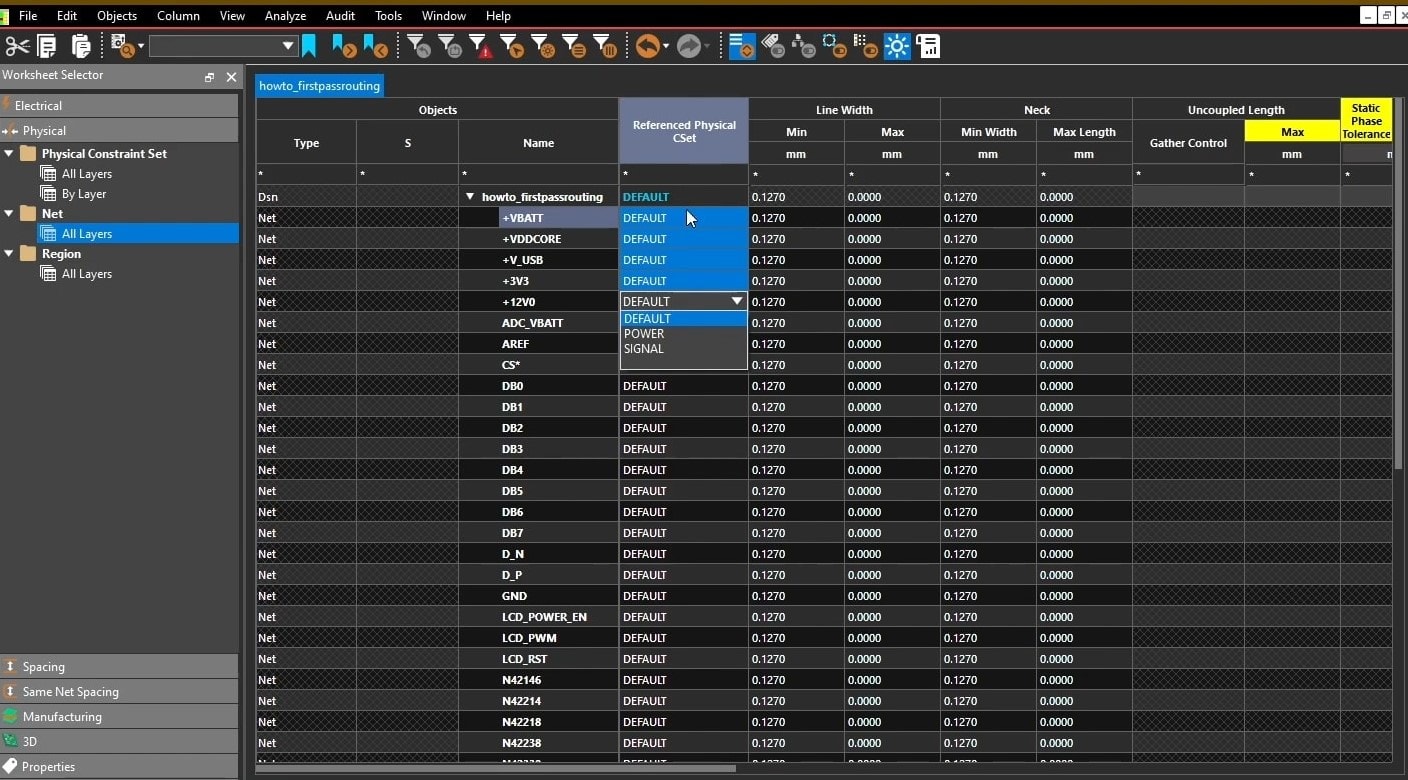
Assigning CSETs to Nets After defining the CSETs, assign them to specific nets. In the Net section, all nets are listed, and you can organize them into groups or buses. This organization simplifies the process of applying CSETs to multiple nets simultaneously. Assign the power CSET to high-power nets, like +VBATT or +VDDCORE, while applying the signal CSET to nets handling data or low-power signals. This step ensures each net follows the required constraints, making it easier to manage and update values if needed.
-
Setting Up Spacing Constraints Spacing constraints are essential for avoiding electrical interference and ensuring proper separation between components. Within Constraint Manager, you can set specific spacing requirements, like the minimum allowable distance between traces or vias. Create spacing CSETs for power and signal nets separately and set spacing values accordingly—0.254 mm for power traces, for instance, and 0.15 mm for signal traces. Assign these CSETs to nets in the Spacing section, ensuring that the design complies with spacing standards across all areas.
Managing Constraints with OrCAD X: Analysis Mode and Additional Rules
OrCAD X allows for enabling and disabling specific rules directly in Constraint Manager. For instance, by right-clicking on constraint headers and selecting Analysis Mode, you can enable real-time rule checking for design rule compliance (DRC) errors. Set rules for vias by choosing allowable via types and specifying clearances, enhancing control over via placements.
Once constraints are defined, OrCAD X offers the flexibility to export these settings as a technology file. This file can be imported into other designs or reused within the current design environment. By exporting to a .tcfx file, designers can share constraint configurations across multiple projects, improving consistency and saving time on repetitive setups.
For high-speed designs, you can also use OrCAD X analysis features to simulate and determine precise trace lengths based on signal timing requirements, enabling advanced control over constraints like differential pairs and serpentine routing.
Assigning the spacing constraint sets in OrCAD X
Effective PCB design constraints management is crucial for ensuring both functionality and manufacturability in modern designs. By establishing and managing design rules early, engineers can prevent signal integrity issues, ensure proper spacing, and streamline the layout process. With Cadence tools, specifically OrCAD X, designers gain access to powerful features like Constraint Manager, which allows them to create, assign, and monitor design constraints with precision. OrCAD’s integration with other Cadence PCB Design and Analysis Software solutions provides a comprehensive environment for creating high-performance, error-free PCBs.
Leading electronics providers rely on Cadence products to optimize power, space, and energy needs for a wide variety of market applications. To learn more about our innovative solutions, talk to our team of experts or subscribe to our YouTube channel.