Using Figure of Merit in Electronic Systems for PCBA Cost-Benefit Analysis
Key Takeaways
-
What is a figure of merit (FOM)?
-
Common FOMs for Electronic Systems.
-
How to create a cost-benefit FOM.
Measuring a comparable metric
Personally, I love football and am in awe of the physical abilities of professional athletes. However, I must admit that the decathlon, where contestants must compete in 10 events, is a more comprehensive evaluation of athleticism. It is worth noting that four of the events are running contests: 100-meter dash, 110-meter hurdles, 400-meter dash, and 1,500-meter run. Coincidence? Perhaps, but not when you consider that a foot race is probably the purest embodiment of physical competition with one easily comparable metric--speed.
The ability to accurately compare attributes and processes is an essential part of PCBA development. During design, components are selected based upon their performance criteria for a certain metric(s), typically available on the datasheet. Manufacturing processes, especially high-volume production, are judged on the ratio of usable boards to boards built--the yield rate. The usefulness of these assessments is dependent upon the metric that is used for the comparison.
Let’s take a look at how this type of metric or figure of merit in electronic systems is used and what is necessary to apply it to cost-benefit analysis.
What is a Figure of Merit in Electronic Systems?
You may be surprised to learn that the term figure of merit (FOM) is not new, nor is its usage in electronic systems. In 1965, H. C. Josephs of Honeywell described how a commonly used metric for digital systems could be expressed in terms of a simple FOM [1]. This application is sufficient to illustrate the underlying purpose of FOM utilization in electronic systems.
A Figure of Merit (FOM) is a determinable metric that defines an electronic component, device, or system in terms of its performance, which can be broadly applied and compared.
This simple but accurate description speaks to the fact that there are no real boundaries on what a FOM can be. Its worth or merit lies in its usability to compare similar devices or systems. Common uses or types of FOMs are listed below:
Types of Figure of Merit for Electronic PCBAs
☐ Component Parameter
One of the most common uses of FOMs is to compare component performance. This usually involves a simple equation comprised of multiple parameters to define a new comparable metric.
☐ Device Parameter
Creating FOMs to compare a performance aspect of different devices can also be useful. For example, a total power loss FOM can be determined to compare different device technologies.
☐ System Parameter
One of the most common metrics for assessing the quality of a system is by comparing usable outputs with applied inputs. For a PCBA manufacturing process, this FOM is the yield rate.
Determining FOMs for Electronic PCBAs
As stated above, FOMs can be quite simple depending upon their usage; the inverse is also true. FOMs can be quite complex as well. A perfectly reasonable question then is, “How do you create a FOM?” This is not an easy question to answer and there is no one-size-fits-all solution. Before offering one up, let’s consider the flowchart below.
Example FOM creation flowchart1
IMG: FOM creation example.jpg in Cadence | Software Images/Figure of Merit.
This chart may seem complicated, however, it does provide a step-by-step process or paradigm for developing a FOM. Albeit this does require teams and time. Even more important than a paradigm, it highlights some of the important questions to be answered for any FOM determination, which are included in the list below:
1Image from “Producibility and Other Figures of Merit” at https://pcb.iconnect007.media/index.php/article/98335/producibility-and-other-figures-of-merit/98338/?skin=pcb. Accessed 6/16/20.
Determining a Figure of Merit
If you can answer YES to all of the questions in this shortlist then you are ready to proceed with your FOM development. Otherwise, you should revisit your development strategy and motivation prior to continuing with the chosen FOM. Now, let’s take a look at what is necessary to develop a FOM for cost-benefit analysis.
PCBA Development Cost-Benefit Analysis Using FOM
The objective of PCBA development is to design, build, and test your boards until the best design is realized to produce and market. This includes optimizing manufacturability and realiblity once in the field. This board development process is cyclical and, therefore, effective engineering prototyping workflow management is essential to control costs. The extent to which direct costs impact your design decisions may vary, yet it is a good bet that the balance between costs and value has a significant impact. This importance level qualifies cost-benefit analysis as a prime candidate for FOM utilization.
Attributes for Cost-Benefit Analysis Figure of Merit
⚖ It must be comprised of independent cost metrics.
⚖ All cost factors must be measurable and/or calculable.
⚖ There must be a clear definable standard (for example, a threshold that separates acceptable from unacceptable) or it must be comparable across different development processes.
Implementing or developing a FOM is most often an external design process, which means additional time and the added probability of errors. A better option is to employ a PCBA design platform that enables cost-effective analysis design.

Cost-effective analysis-driven design with Allegro
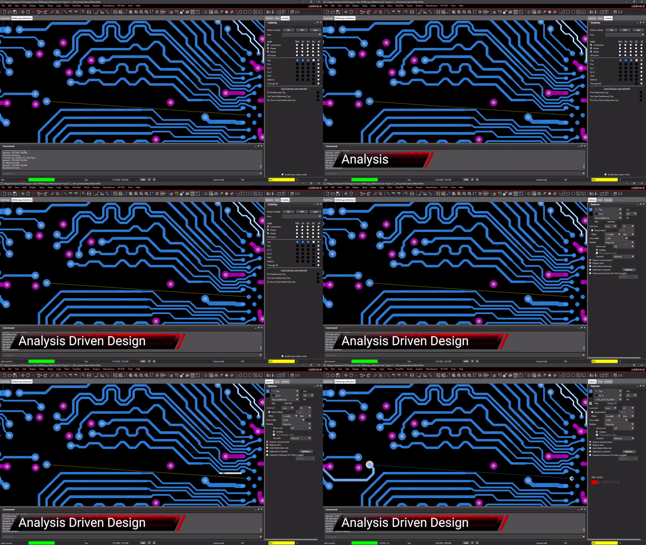
As the clip illustrates, with Allegro you can employ analysis-driven design to eliminate post-design rework and improve the cost-effectiveness of your development process.
Cadence’s PCB Design and Analysis package is the most advanced and comprehensive in the industry. And by taking advantage of the advanced capabilities of Allegro, including In-Design Analysis (IDA), you can develop and monitor your cost-benefit metrics.
If you’re looking to learn more about how Cadence has the solution for you, talk to us and our team of experts.
References
1. Josephs, H. C. , “A figure of merit for digital systems,” Microelectronics Reliability 4, no. 4 (December 1965): 345-350, https://doi.org/10.1016/0026-2714(65)90171-X.