The Seven Best Reasons for Being a Circuit Board (PCB) Designer
Key Takeaways
-
Why circuit board design is such a rewarding career.
-
The professional and personal growth you can experience as a PCB Designer.
-
Not only do you design next-generation electronics, but you get to use the most advanced tools.
PCB design collaboration.
I know a lot of people who dread facing a new workday, but thankfully, that isn’t the case for me. Sure, there are times when I’m tired or things just aren’t going very well and I would rather be anywhere else than at work. For the most part, though, I really enjoy what I do and I look forward to it each day. I think the reason for this is because I design printed circuit boards, and in this job, there is always something new coming around the next bend in the road.
Although this job has its regular routines and schedules like any other job, the variety of the electronic designs that I have worked on has always kept me on my toes. I’ve worked on some of the smallest designs for wearable IoT devices, large boards for industrial power applications, and just about everything else between. Not many careers offer this amount of diversity in what a person can do, and that is just one of the benefits of a career in circuit board design. Here are seven reasons why designing circuit boards is one of the best jobs you can have.
Seven Reasons Why Circuit Board Design is Such a Rewarding Career
Working with a variety of electronic devices
One of the greatest joys of my career as a circuit board designer is getting to use some of the products that I have designed boards for. Whether for personal or professional use, it is a feeling of immense satisfaction to flip the switch and see the device that I had a part in creating come to life. I have also designed boards for avionics, communications, and medical equipment. And, knowing that I have contributed towards keeping people safe and healthy is also very rewarding. The number of applications for circuit boards in today’s electronics is limitless, and there are always new and interesting products for PCB designers to work on.
Designing the latest cutting-edge technology
As the need for electronic devices grows, their complexity continues to increase while their size decreases. What this means for the PCB designer is that there are plenty of new technological challenges waiting for you to tackle. For the devices we build to get smaller, the designs must get smaller and more densely packed as well. This requires new techniques and methods in circuit board design, and the PCB designer is on the front lines of these new requirements.
Working in 3-D is just one of the new techniques and methodologies in PCB design.
Associating with some of the world’s brightest and most interesting people
There are many designers all over the world that face the same sort of challenges, and fortunately, there are plenty of resources available to network everyone together. There are blogs like this one as well as research papers and webinars to share information. There are also small and large designer groups in different areas that host meetings and events to keep everyone informed. PCB designers love to talk about their work, and there is nothing better than being able to spend some time with other industry professionals at a design conference to learn and share experiences.
You get to talk about the most interesting topics
Not only can you talk fluently about circuit boards as a PCB designer but you also will have a wide association with many other areas of interest. For instance, if you are designing circuit boards for autonomous vehicle systems, you probably will have a fair amount of knowledge about those systems and cars, in general, to go along with it. This puts PCB designers in the driver’s seat, so to speak, as far as being able to engage with many people on multiple subjects. If nothing else, you are sure to be an expert on setting up and using a computer, which will make you everyone’s best friend at one point or another.
You can also end a conversation as quickly as you need to
On the flip-side, you also will have a built-in defensive mechanism to help you get out of social events that you feel trapped in. I can guarantee you that by switching topics to the merits of mechanically drilled vias versus laser-drilled vias you will be able to kill any casual conversation that you are part of giving you an easy escape. This one comes in handy more often than you might expect.
Placing components and routing traces is just plain fun
Being able to place components on the screen of your PCB design system and then maneuver them around to the most optimal position is a lot of fun. Then, on top of that, you get to connect all of the nets together by routing traces to each component pin. With so many pieces to fit together, it’s like working with a giant puzzle. And when this particular puzzle is completed as a finished printed circuit board, it brings with it an incredible sense of accomplishment.
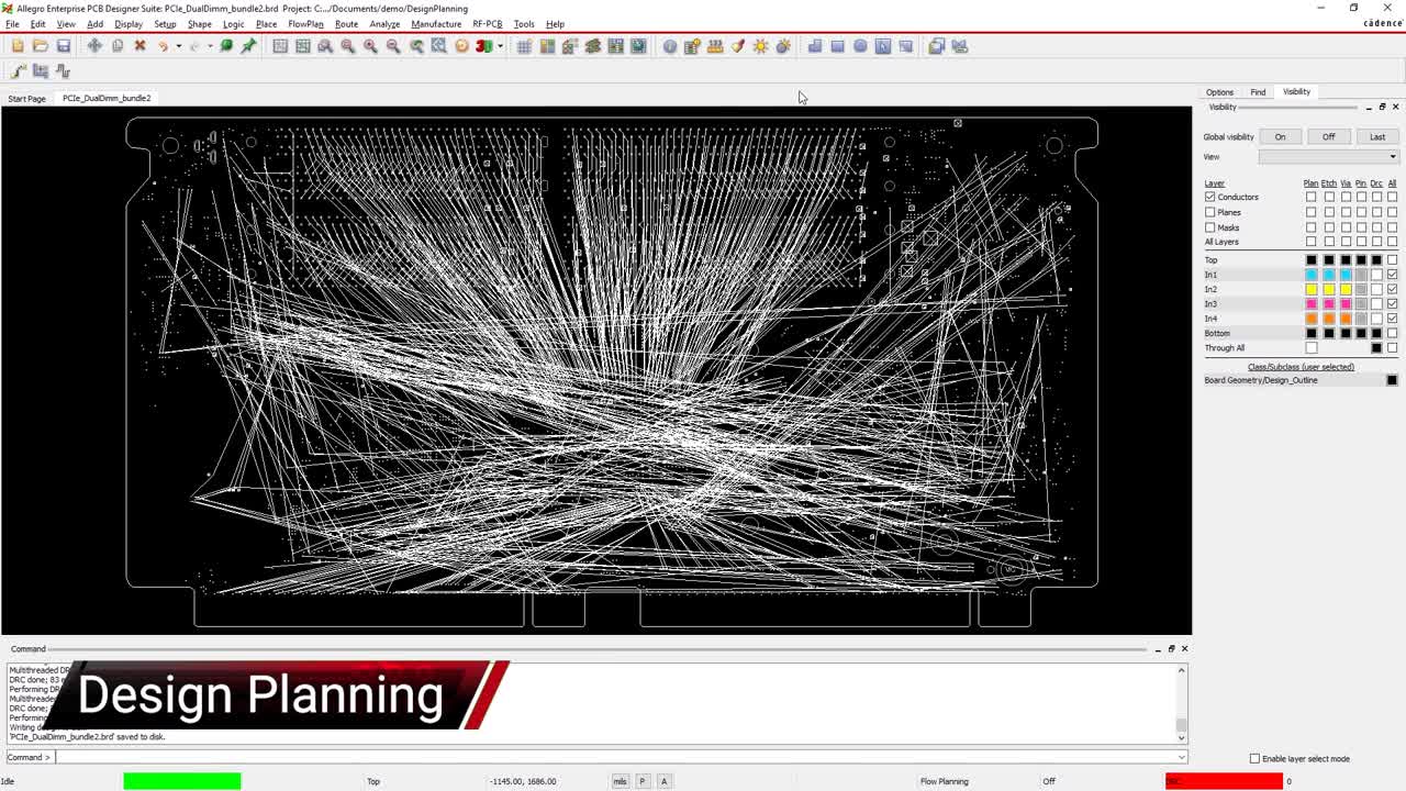
You get to work with some of the most advanced software around
PCB design tools have grown and evolved through the years to provide the best capabilities for their users to do their jobs. As a PCB designer, you will be using these tools to capture complex schematics, and lay out intricate printed circuit boards. These tools are a far cry from a simple drawing instrument though. Instead, they have an incredible amount of functionality built into them so that you can design your electronics with precision and accuracy. While circuit designs have continued to grow in complexity over the years, design tools have continuously evolved to make your life easier, letting you tackle the bigger problems.
Using advanced 3-D technology like this will help with precision and accuracy in PCB design.
What’s the Next Step?
There are many paths to becoming a printed circuit board designer but the most obvious one is to study electrical engineering in school. Once you are ready, though, you too will be able to start with the basic steps of designing and laying out advanced electronics with PCB design tools.
The key to all of this is working with a PCB design system that can not only handle the most complex designs but also help new users come up to speed quickly on using CAD tools. One of the best systems for this is OrCAD PCB Designer from Cadence. It has the tools and functionality to expertly take you all the way through the design cycle while helping you to learn and grow along the way.
If you’re looking to learn more about how Cadence has the solution for you, talk to us and our team of experts.